A thyristor is a semiconductor device that belongs to the family of four-layer, three-junction semiconductor devices. It is a type of electronic switch that can control the flow of electrical current in a circuit.
Thyristors are known for their ability to switch high voltages and currents, making them useful in a wide range of applications, including power control and electronic switching.
Thyristors
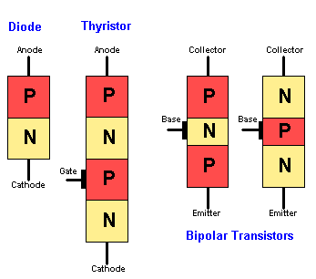
A thyristor (a pnpn device) is a member of the transistor (pnp or npn) family from the perspective of construction. The word “thyristor” is made up of the capital letters THYRatron and transISTOR. As a result, thyristors are solid-state devices like transistors with properties resembling those of thyristor tubes.
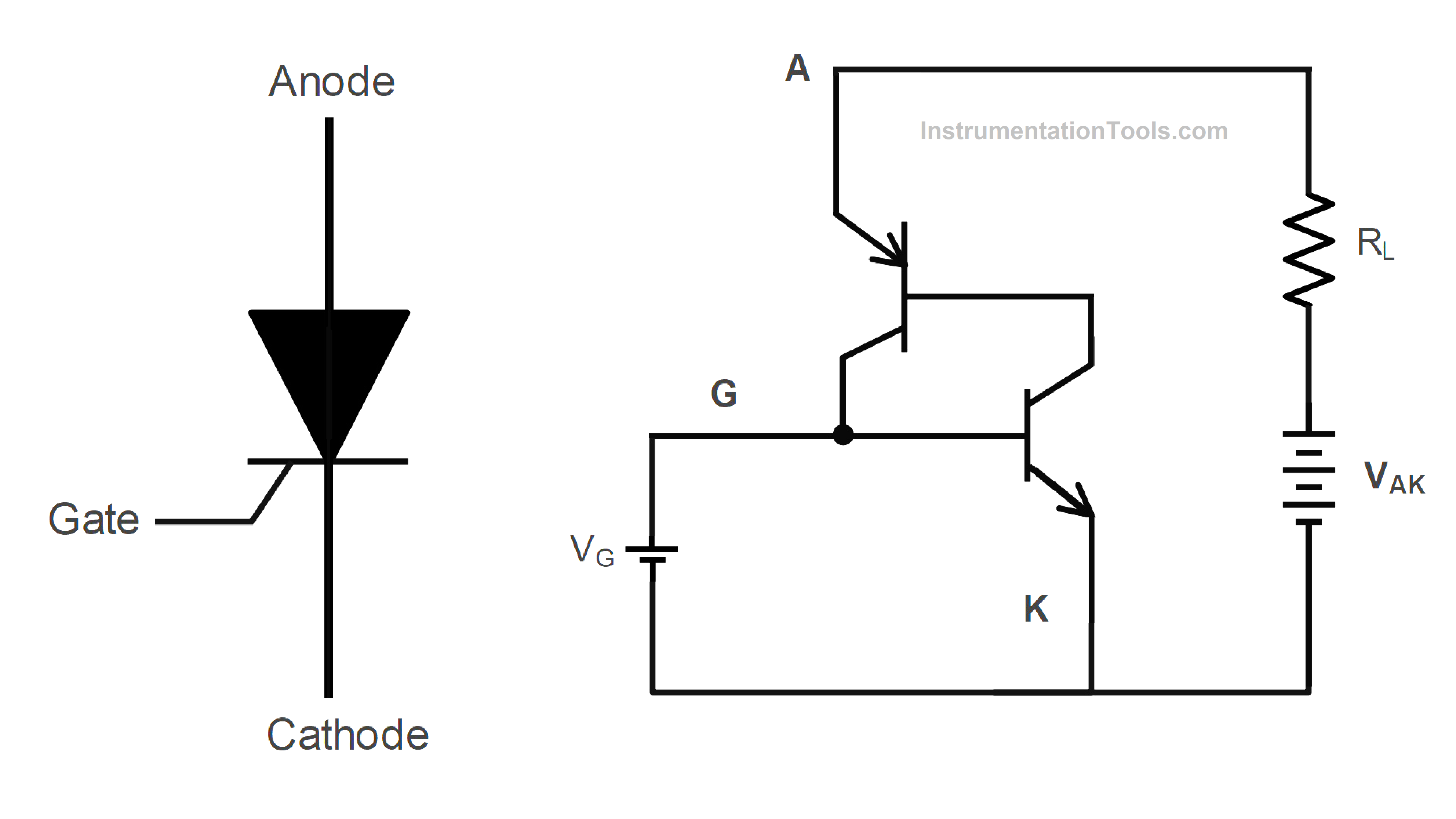
Fig 1. Thyristor Symbol and Equivalent Circuit
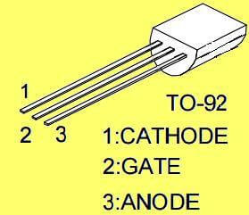
Thyristors’ terminal characteristics distinguish them from other semiconductor devices like diodes and transistors. The main terminal of the thyristor is the Anode (A), Cathode (K) and Gate(G).
Anode (A): The anode is the positive terminal of a thyristor. It is where the current enters the device when the thyristor is in its forward-biased conducting state.
Cathode (K): The cathode is the negative terminal of a thyristor. It is where the current exits the device when the thyristor is in its forward-biased conducting state.
Gate (G): The gate terminal is used to control the thyristor’s conduction. Applying a small current or voltage pulse to the gate terminal triggers the thyristor into its conducting state. Once triggered, the thyristor remains in the conducting state until the current flowing between the anode and cathode falls below a certain threshold, or until a reverse voltage is applied across the anode and cathode.
Working Principle of Thyristor
The thyristor is a three-terminal device namely Anode (A), Cathode (K), and gate (G), and a four-layer device PNPN. The terminal connected to the outer p-region is called Anode (A) and a terminal connected to the outer n-region is called Cathode (K). The inner region of p-layer is connected with the terminal Gate (G).
There are three modes of operation of Thyristor (i) Reverse blocking mode (ii) Forward blocking mode and (iii) Forward Conduction mode. In the detailed mode of operation, we can look at the Static VI characteristics of the thyristor.
The Load (RL) gets the current when the device is turned on. The device will be on either in the absence of gate voltage or in the presence of the gate voltage. But it is recommended to turn on the thyristor using gate voltage. In the absence of gate voltage, very high Anode to Cathode voltage is required. So, it is better to lessen the anode-to-cathode voltage and give a short pulse of gate voltage to turn on the device.
The Layer diagram and Circuit schematic of the Thyristor is shown below. In the below Fig the gate voltage is provided with a switch for the above condition.
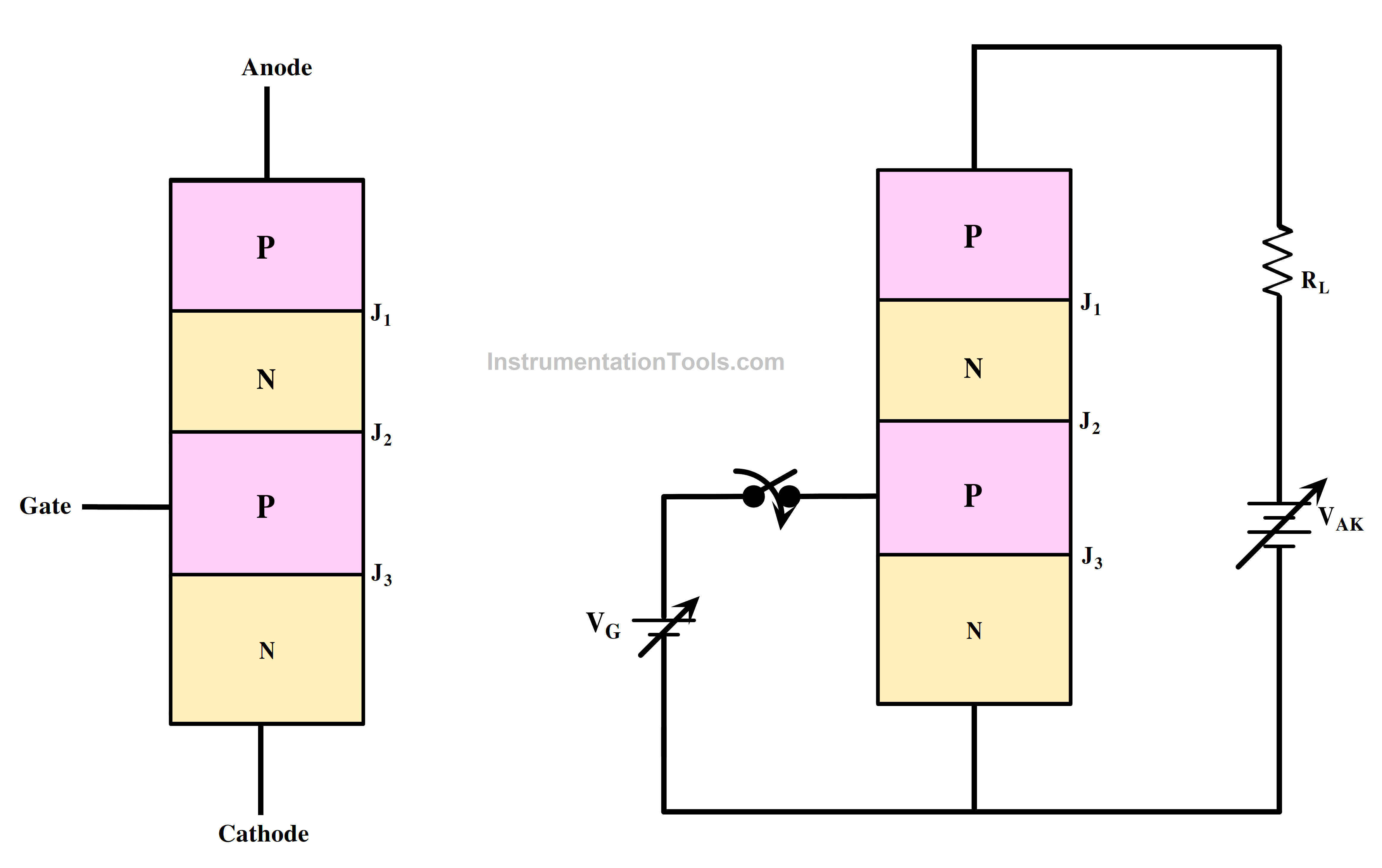
Fig 2. Thyristor Layer Diagram (Left) and Biasing Circuit (Right)
The thyristor can be triggered into the on state by applying a gate current (Ig) that exceeds a specific threshold. This triggering process is often accomplished using one of the following methods:
Forward Biasing: By applying a positive voltage to the gate with respect to the cathode, which allows current to flow from the anode to the cathode.
Gate Current Pulse: Applying a short pulse of current to the gate terminal to trigger the thyristor.
Static VI Characteristics of Thyristors
The VI Characteristics of Thyristor are explained below. The VI characteristics explain the working of thyristor for different modes of operation mentioned above.
The graph is plotted between Anode to Cathode Voltage (VAK) and Anode Current (Ia).
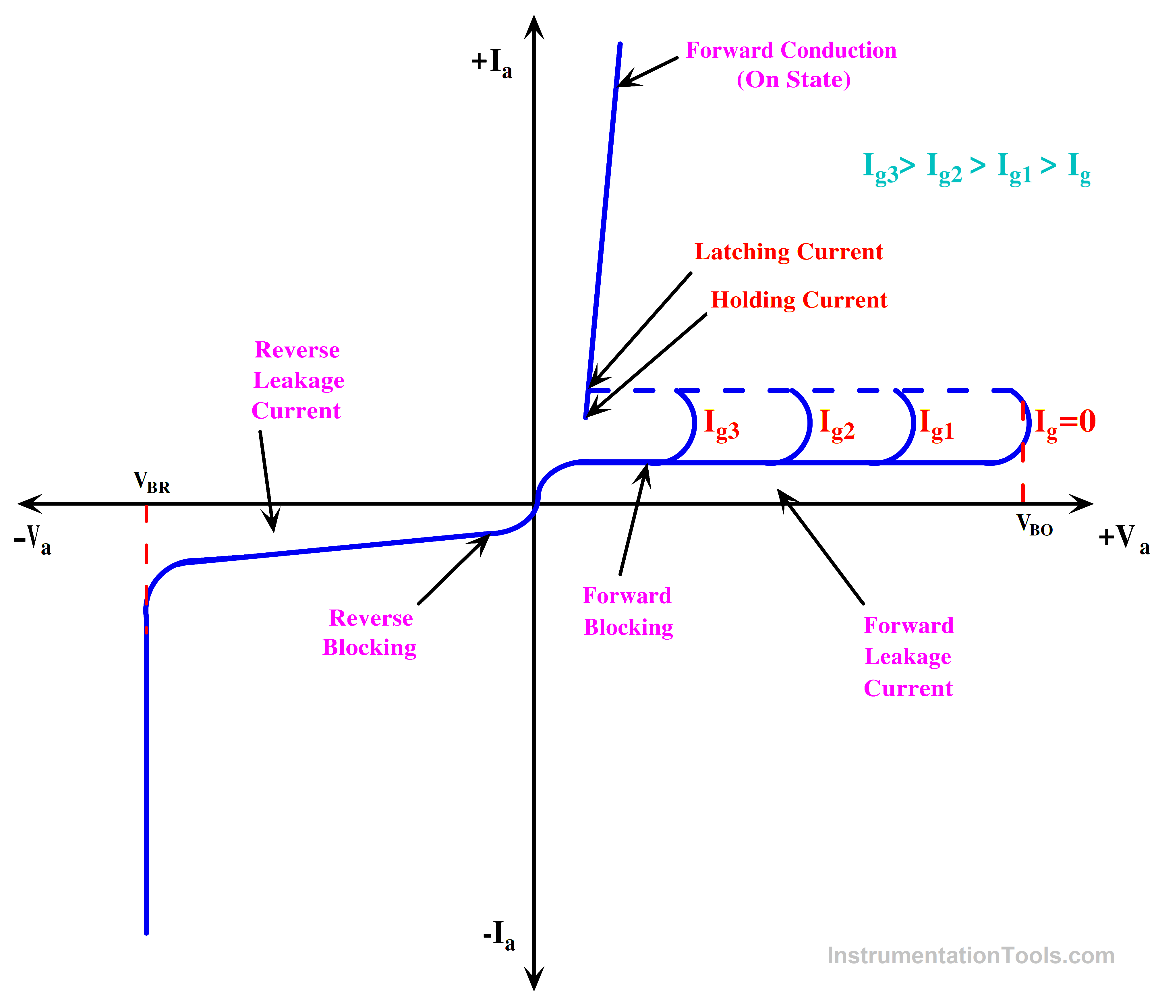
Fig 3. Static VI Characteristics of Thyristor
The three modes of operation of thyristor are
- Reverse blocking mode
- Forward blocking mode(Off Mode)
- Forward Conduction mode(ON Mode)
Reverse Blocking Mode
The reverse blocking mode of a thyristor refers to the condition in which the thyristor is blocking current flow in the reverse direction, meaning it is not allowing current to pass from the anode to the cathode.
In the reverse blocking mode, the thyristor is reverse-biased, which means the voltage applied across the anode and cathode terminals is such that the anode is at a lower potential than the cathode. The cathode is Positive and Anode is Negative. This reverse bias voltage prevents the thyristor from turning on or conducting current in the forward direction.
Since Thyristor has three junctions, during this period Junctions J1 & J3 are Reverse biased and J2 becomes Forward biased. In this mode, the thyristor is in a high-impedance state, which means it has a very high resistance to the flow of current in the reverse direction. Basically, it functions as an open circuit.
If the reverse voltage exceeds a certain critical value known as the reverse breakdown voltage VBR(also called the reverse avalanche voltage), the thyristor may break down and allow a reverse current to flow shown in Fig 3. This can damage the thyristor if not properly protected.
To turn off a thyristor that is in the reverse blocking mode, a negative voltage pulse is applied to the gate terminal. This pulse should have sufficient amplitude and duration to trigger the thyristor into a forward-blocking state. Once triggered, the thyristor can be turned on in the forward direction by applying a forward voltage.
Forward Blocking Mode of thyristor
The term “Forward Blocking Mode” typically refers to the behavior of a thyristor when it is in a non-conducting state in response to a forward voltage applied across its terminals. In this mode, the thyristor is not conducting current, even though a forward voltage is applied across its anode and cathode terminals.
The thyristor remains non-conductive until a specific triggering condition is met. During this mode, the thyristor blocks the voltage applied across its terminals. It acts like an open switch, preventing current flow in the forward direction
During this period Junctions J1 & J3 are forward biased and J2 becomes reverse Biased. In this mode, a small forward leakage is called a forward leakage current. Still, the device can be conducted if the Anode to Cathode voltage is increased. At junction J2 avalanche breakdown occurs called Forward break over voltage VBO. When forward voltage is less than VBO the device offers a high impedance state.
Forward Conduction Mode
A voltage greater than the forward breakover voltage (VBO) or the forward blocking voltage (VDRM) is applied across the thyristor. This voltage should be applied between the anode and cathode terminals. The thyristor must be properly triggered to enter the conduction mode. Triggering is typically achieved by applying a positive pulse or current to the thyristor’s gate terminal. This gate signal initiates the switching process.
During this period a sufficient Anode to Cathode voltage is given with Gate voltage. Junctions J1 & J3 are biased and J2 becomes forward-biased due to the Positive gate voltage.
Once triggered, the anode-cathode voltage must be sufficient to maintain the thyristor in the conducting state. The thyristor will continue to conduct as long as the anode voltage remains above a certain threshold called the forward voltage drop (VF).
As the thyristor enters the forward conduction mode, it becomes a low-resistance path for current flow from the anode to the cathode. The thyristor’s forward conduction mode is characterized by a very low voltage drop (VF) across the device, making it an efficient choice for applications requiring high-current rectification and voltage control.
Different Turn-ON Methods of Thyristor
Thyristors can be turned on using different methods, depending on the specific application and requirements. During this condition the Anode (A) is positive and Cathode (K) is Negative with Gate (G) Voltage applied.
The primary methods for turning on a thyristor are:
- Forward Voltage Triggering
- Gate Triggering
- Light Triggering(LASCR)
- dv/dt Triggering
- Temperature Triggering
Forward Voltage Triggering
The Forward Voltage Triggering method for turning ON a thyristor is a popular way. It involves applying a forward voltage (positive voltage) across the anode and cathode terminals of the thyristor. During this period Junctions J1 & J3 are biased and J2 becomes reverse Biased.
When the voltage exceeds the thyristor’s forward breakover voltage (VBO), the thyristor starts to conduct. It is important to note that this method alone is not always sufficient, as the thyristor may require additional triggering to ensure it switches on reliably.
Gate Triggering
Gate triggering is a precise and controlled method for turning on a thyristor. It involves applying a positive current pulse to the gate terminal while a forward voltage is applied across the anode and cathode.
The gate current pulse can be of sufficient magnitude and duration to initiate conduction. Gate triggering provides precise control over when the thyristor switches on and is commonly used in applications where accurate timing and control are essential.
During this period a sufficient Anode to Cathode voltage is given with Gate voltage. Junctions J1 & J3 are forward-biased and J2 becomes forward-biased due to the Positive gate voltage. Once the device starts conduction the gate loses its control and continues to maintain the conduction even in the absence of gate voltage. The thyristor can be turned off only by reducing the forward current below the threshold called Holding Current.
The holding current is the minimum anode current (also known as anode current or load current) that must flow through the thyristor to keep it in the conducting or “on” state after it has been triggered. It ensures that the thyristor remains in the conducting state until the load current naturally decreases below the holding current due to external factors like load conditions. The typical value of the holding current is a lower value than the latching current and is specified by the thyristor’s manufacturer. It can range from a few milliamperes to several amperes depending on the specific thyristor’s characteristics.
Once the device moves to the conduction state. The gate loses its control and further no need to maintain the gate voltage. The point at which the thyristor moves to the conduction state is called Latching Current.
The Latching current is the minimum gate current (also known as gate trigger current) required to initially turn on the thyristor and transition it from the “off” state to the conducting or “on” state. It is the current level needed to trigger the thyristor and start the conduction process. Once triggered, the thyristor will continue to conduct until the load current falls below the holding current.
The typical Value of the latching current is higher than the holding current and is also specified by the thyristor’s manufacturer. It can range from a few milliamperes to several amperes, depending on the specific thyristor’s characteristics
Light Triggering (Optical Triggering)
Thyristors can be triggered using light, typically through a process called phototransistor triggering or opto-isolation. A light-sensitive device, such as a phototransistor or photodiode, is used to detect a specific light signal and then generate a current or voltage pulse to trigger the thyristor.
This method is often used in isolation and control circuits, where electrical isolation is required between the triggering circuit and the thyristor.
Voltage Rate of Change (dv/dt) Triggering
Thyristors can also be turned on by rapidly increasing the voltage (dv/dt) applied across their terminals. When the rate of change of voltage exceeds a certain threshold, the thyristor may trigger unintentionally. Care must be taken to avoid unintended triggering in high dv/dt environments.
Consider the Cj junction’s capacitance. For every capacitor, If it is assumed that all of the forward current va passes through the reverse biased junction j2, then the charging current through the junction is provided by. In some applications, special dv/dt protection circuits are used to prevent false triggering.
Temperature Triggering (Thermal Runaway)
In rare cases, thyristors can be triggered by an increase in temperature due to a high current or other factor. This is not a desirable method for controlled triggering and should be avoided in most applications. Proper thermal management and protection measures should be in place to prevent unintentional triggering due to thermal effects.
The choice of thyristor turn-on method depends on the specific requirements of the application, including the need for precision, speed, isolation, and reliability. Gate triggering is often preferred when precise control is required, while forward voltage triggering is simpler but may be less precise.
Other methods like light triggering and dv/dt triggering have their own niche applications where electrical isolation or unique triggering conditions are necessary.
Reference
- “ Power Electronics” P. S. Bimbhra, Khanna Publishers, 2012
- “Power Electronics: Circuits, Devices and Applications“, M H Rashid, Pearson Education
If you liked this article, then please subscribe to our YouTube Channel for Instrumentation, Electrical, PLC, and SCADA video tutorials.
You can also follow us on Facebook and Twitter to receive daily updates.
Read Next:
- Power MOSFET – Symbol, Types
- How to test SCR using a Multimeter
- MCT (MOS Controlled Thyristor)
- SCR Triggering Methods Explained
- Types of Power Electronic Devices