What is a transistor and types of transistors?
Transistor is a semiconductor device capable of transferring the signal from high resistance to low resistance or vice versa. Transistor has three terminals and is used in electronic circuits as amplifiers and switches. There are mainly three types of transistors used in electronic circuits they are a) bipolar junction transistor b) Junction field effect transistor c) Metal oxide semiconductor field effect transistor.
What is bipolar junction transistor?
The name Bipolar came from the fact that the device operation depends on movement of charge carriers with both polarities (holes and electrons). BJT has three terminals a) Emitter b) base c) collector analogous to cathode gate and anode in vacuum tube. Emitter is heavily doped collector is moderately doped and base is lightly doped as we need most of the current from emitter should reach collector; base current is needed only as a pilot signal for collector current variation. Transistor is active device which has the ability to control the electron flow through it. BJT is of two types 1) PNP transistor 2) NPN transistor .PNP transistor is formed by sandwiching n-type semiconductor between two P-type semiconductors. Similarly PNP transistor is formed by sandwiching n-type semiconductor between two P type semiconductors.
What is power dissipated by transistor in active region?
The power dissipation across the transistor mainly occurs at the collector junction. This is due to the fact that the collector junction is reverse biased, so offers more resistance to current flow. Hence more voltage drop occurs across the collector junction. Power dissipation across the transistor is given by
{ VBE is neglected as VBE << VCE }
Why inverse active mode of transistor is not useful?
Bipolar junction transistor internal design is in such a way that it will have high gain in normal active mode. Also when you interchange the roles of emitter and collector with emitter base junction reverse biased then break down voltage decreases as break down voltage is inversely proportional to the amount of doping. As emitter is highly doped compared to collector it is advantageous to reverse bias collector base junction in order to have the advantage of high breakdown voltages.
What are the types of transistor configurations?
BJT can be operated in three configurations with one terminal common to both input and output. They are a) Common Base b) Common emitter c) Common collector configurations.
What are α,β and γ in a transistor ?
β is current gain of transistor in common emitter configuration. Common emitter current gain beta (β) = Ic/Ib as in common emitter configuration input current isIb and output current is Ic. α is large signal current gain of transistor in common base configuration α = (Ic –Ico) / (IE-0). Alpha typically varies from 0.9 to 0.995.If we neglect reverse saturation current Ico then beta can be represented in terms of alpha, β= α / (1- α). In common collector configuration output is taken at emitter terminal, hence common collector current gain is given γ = IE/IB (input current is IB and output current is IE). γ is also called emitter injection ratio.
What is the relation between α,β and γ in a transistor?
α*β*γ=1.
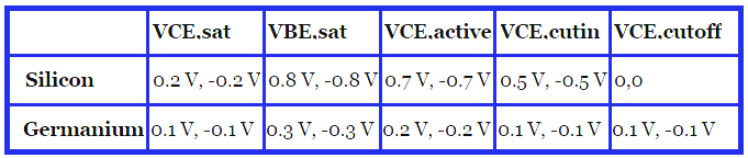
What are the values of collector to emitter, Base to emitter saturation, active, cut in, cut off voltages?
Typical n-p-n, p-n-p transistor junction voltages at 25 Deg C
What is ICBO and ICEO in a transistor what is relation between ICEO,ICBO and ICO?
ICBO is the collector current with collector junction reverse biased and base open-circuited. ICEO is the collector current with collector junction reverse biased and emitter open-circuited.
Why ICBO is greater than ICO?
ICBO is greater than ICO for two reasons
- In addition to the reverse current through the junction, there exists a leakage current which flows around the junction and across the surfaces.Ileak α Vjunction
- New carriers may be generated by collision in the collector junction transition region.
What are the different regions of operation of transistor?
In BJT due to the presence of two junctions, each junction can be operated in forward or reverse bias leading to three different regions of operation. Transistor when used as a switch in logic gates will be operated in extreme regions of input output characteristics in which both regions will be forward biased or reverse biased which are called saturation and cut off regions of operation simultaneously. Transistor when used as amplifier is operated in active region in which input junction will be forward biased and output junction will be reverse biased. Other region inverse active region is of less importance in practice.
What is Ebers model of transistor?
Ebers-moll model of transistor holds for all regions of operation of BJT. This model is based on assumption that base spreading resistance can be neglected.
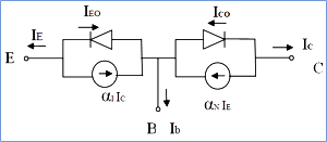
Consider a diode with voltage v applied between its terminals. The current flowing through the junction in terms of applied voltage between its terminals is given by
I=Io (exp (V/Vt)-1)
Where Io is reverse saturation current of the transistor (Current which flows across junction when it is reverse biased will be –Io as exp (V/Vt) tends to 0).From the diagram applying Kirchhoff’s current law at the collector node, we get
Ic = –αNIE+Ico (exp (VBC/Vt)-1)
Where αN is the current gain of common base transistor mentioned above, VBC is the base to collector voltage, Ico is the reverse saturation current of base collector junction. Similarly for emitter junction by applying Kirchhoff’s current law
IE= –αIIC+IEo (exp (VBE/Vt)-1)
Where αI is the inverted current gain of common base transistor with roles of collector and emitter interchanged, VBE is the base to Emitter voltage, Ico is the reverse saturation current of base Emitter junction. The above equations are derived based on the assumption of low level minority carrier injection (the hole concentration injected into the base is very much less compared to the intrinsic electron concentration in base), in such a case emitter or collector current is mainly dominated by diffusion currents, drift current is negligible compared to drift currents.
How to obtain response of transistor to large signal and small signals?
A Bipolar Junction transistor acts as a nonlinear device if input-output voltage swing is large. In such a case large signal response of a transistor is obtained graphically. But for small signals transistor operates with reasonable linearity so that the small signal response of the transistor can be obtained analytically by using model of transistor. These small signal transistor models are small signal approximations of transistor in linear active region. The notion of small signal is valid for voltages of the order of milli volts around the bias point.
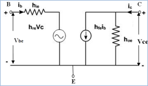
Small signal hybrid model of transistor?
The basic two port equations for transistor in common emitter configuration are
Vbe = hfe*ib + hre*Vce
ic = hfe*ib + hre*Vce
Where Vbe, ib, Vce, ic are incremental currents and voltages (incremental means for example ib=Ib–IB where Ib is instantaneous base current, IB is quiescent base current)
Define Transconductance of a transistor?
The Transconductance of transistor is defined as the ratio of incremental collector current to incremental base to emitter voltage with collector to emitter kept constant. It is denoted by gm.
gm= |Ic|/VT
where VT = K*T/Q = 26 milli volts at room temperature of 27 Deg C,
gm= |Ic(mA)|/26.
Small signal PI model of transistor?
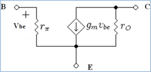
Where gm = |Ic (mA)|/26, rΠ = β / gm, rO = VA / Ic where β is small signal current gain in common emitter configuration, VA is Early voltage, Ic is collector current, Vbe is incremental base to emitter voltage.
Small signal T model of transistor?
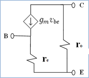
Where gm = |Ic (mA)|/26, re = α / gm, rO = VA / Ic
where α is small signal current gain in common base configuration α = β/(1+ β), β is small signal current gain in common emitter configuration, VA is Early voltage, Ic is collector current, Vbe is incremental base to emitter voltage. The relation between re and rΠ is rΠ = (1+ β)* re.
What is Q point?
Q-point is an acronym for quiescent point. Q-point is the operating point of the transistor (IC,VCE) at which it is biased. The concept of Q-point is used when transistor act as an amplifying device. Q-point is generally taken to be the intersection point of load line with the output characteristics of the transistor. There can be infinite number of intersection points but q-point is selected in such a way that irrespective of input swing transistor remain in active region. All the input AC signals variations happen around Q-point.
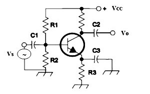
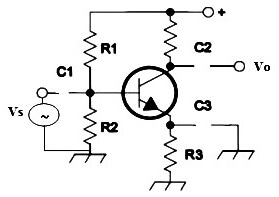
What is self bias (or) voltage divide bias circuit of transistor?
The name self bias is coined because of the fact all the DC variations around Q-point tends to adjust itself in self bias circuit. The self bias circuit is shown below
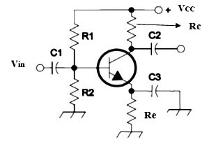
All the capacitors shown in the figure acts as open circuit for DC and short circuit for AC signals. The self bias action can be explained as follows If Ic tends to increases due to increase in Ico (due to increase in temperature) the current through Re also increases. As a result voltage drop across Re also increases, hence base to emitter voltage decreases and base current decreases. Hence Ic increases less due to the action of self biasing resistor Re.
Stability factor S = 1 + (Rb/Re) Where Rb = (R1*R2)/(R1+R2)
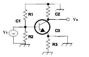
What is fixed bias?
The fixed bias circuit is shown in figure below: Transistor fixed bias circuit
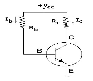
Current Ib is constant in fixed bias circuit. The Fixed bias circuit offer poor stability w.r.to variation in transistor parameters. In fixed bias circuit
Stability factor S = 1+β
Define stability factors of a transistor operated at Q-Point?
The main aim of biasing circuits is to stabilise the transistor’s operating point irrespective of variations in Ico, β, Vbe which vary because of varying temperature. Mainly the variation of Ico with temperature is a significant one and has to be taken care of. Accordingly a stability factor is defined o quantify the stability of biasing circuits with respect to variation in transistor parameters.
Stability Factor S = Ic/ Ico
Similarly S’ = Ic/ β, S’’= Ic/ Vbe
What is thermal resistance of a transistor?
Thermal resistance is defined as the ration of steady state temperature raise at the collector junction to the power dissipated at the junction. It is expressed in Deg C/W and is given as
Φ = (Tj-TA)/ PD
What is base width modulation or earlier effect?
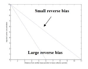
Consider a transistor in common base configuration biased in active region of operation. As you increase collector to base voltage that is if you more reverse bias base collector junction the depletion layer width increases as depletion layer width is proportional to reverse bias voltage. This depletion layer protrudes more in to the base than collector because base is lightly doped compared to collector. As we increase base to collector voltage depletion layer width increases this in turn decreases effective base width. According to law of junction injected carrier concentration in base should reduce to zero at the onset of depletion layer in base. In the graph(plotted with minority carrier concentration on Y-axis anddistance from emitter base junction to base collector junction on x-axis stands) shown below the left side is plotted for higher reverse bias compared to graph on right side with less slope compared to the one on the right .This is termed as Early effect.
Effects of the base width modulation?
Base width modulation (or) Early Effect has three main consequences
1. As emitter current is mainly diffusion current (assuming low level injection) now as collector base reverse bias increases hole concentration gradient increases, this leads to more emitter current (IE α ∆P/∆X).
2. Also as effective base width decreases there is less chance for recombination and base current decreases as reverse bias increases a base is mainly due to recombination currents, so beta current gain of common emitter transistor increases.
3. As we increase further the reverse bias voltage at some point effective base width approaches zero and transistor will breakdown .This phenomenon is called reach through or punch through.
What is high frequency model of transistor?
At high frequencies the low frequency small signal model of transistor has to be modified to include the effect of parasitic capacitances of transistor. Following is the high frequency model of a transistor.
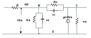
Where
B’ = internal node in base
Rbb’ = Base spreading resistance
Rb’e = Internal base node to emitter resistance
Ce = Diffusion capacitance of emitter base junction
Rb’e = Feedback resistance from internal base node to collector node
Gm = Transconductance
CC= transient capacitance of base collector junction
Express high frequency model parameters of a transistor in terms of small signal low frequency hybrid parameters?
Transconductance gm = Ic/Vt
Internal Base node to emitter resistance rb’e = hfe/ gm = (hfe* Vt )/ Ic
Internal Base node to collector resistance rb’e = (hre* rb’c) / (1- hre) assuminghre << 1 it reduces to rb’e = (hre* rb’c)
Base spreading resistance rbb’ = hie – rb’e = hie – (hfe* Vt )/ Ic
Collector to emitter resistance rce = 1 / ( hoe – (1+ hfe)/rb’c)
What is the relation between large signal current gain (or) DC current gain and small signal beta?
The DC current gain is defined as the ratio of collector current to base current whereas small signal gain is the ratio of incremental change in collector current to the incremental change in base current.
DC current gain βdc = Ic/Ib, small signal current gain β = hfe = Ic/ Ib at constant Vce
Since Ic = β*Ib + (1+β)*Icbo differentiating and rearranging the terms we get
β = βdc/(1-(( Icbo+ Ib)* βdc / Ic))
Where Icbo is reverse saturation current with surface currents e.t.c taken into account.
Why two back to back diodes cannot function as a transistor?
Consider two diodes connected back to back in the configuration shown below
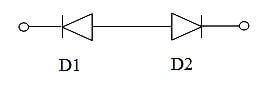
It is obvious that if one junction is forward biased then other junction will be reverse biased consider for example diode D1 is forward biased and diode D2 is reverse biased much like a NPN transistor in active region according to the junction voltages only current order of reverse saturation current flows through the series junctions.
This can be explained as follows: the reverse biased diode D2 at most will allow only currents order of reverse saturation currents. Since D1 and D2 are in series only currents order of reverse saturation currents flow through their junctions. It is obvious that this is not the case with the transistor in active region (because of the internal design of transistor). The forward current entering the base is sweeped across into collector by the electric filed generated by the reverse bias voltage applied across the base collector junction.
What is punch through in transistor?
As we increase the reverse bias voltage of base collector junction depletion width increases and effective base width decreases (since base is less doped compared to collector, depletion layer protrudes more into the base the collector hence effective base width gets affected), at some point effective base width approaches zero and transistor will breakdown .This phenomenon is calledreach through or punch through.
What is the relation between BVcbo and BVceo?
ANS: BVcbo and BVceo are collector to base breakdown voltage with emitter open circuited and collector to base breakdown voltage with emitter open circuited. The relation between BVcbo and BVceo is
BVceo = BVcbo*(1/ βdc)^n
Where βdc is DC current gain and n is a constant ranging from 2 to 10.
What is significance of avalanche multiplication factor in transistor?
Avalanche Breakdown occurs due to avalanche multiplication of charge carriers. The reverse saturation current that crosses collector junction i.e. Ico becomes M*Ico where M is avalanche multiplication factor multiplied due to avalanche effect. If reverse bias voltage is increased much beyond BVcbo then the avalanche multiplication factor becomes infinitely large and hence the current through the transistor rises abruptly. Avalanche multiplication factor is a function of voltage between collector and base and is given by
M= 1 / (1-(Vcb /BVcbo)^n)
where BVcbo is collector to base breakdown voltages with emitter open circuited
What is signification of emitter degeneration resistance?
ANS: Emitter degeneration resistance refers to addition of resistance in emitter lead which introduces negative feedback in the amplifier circuit. Some of the significant consequences of adding Emitter degeneration resistance are
a) The voltage gain decreases (output is taken across collector) hence the name degeneration resistance (loss in gain). But gain is more stable with respect to variation in transistor parameters. Due to reduction in voltage gain the allowable input signal excursion is large than the one without emitter resistance before the amplifier enters into nonlinear regime.
b) Bandwidth increases. This is because gain bandwidth product remains constant.
c) Input resistance increases.
d) Non linear distortion and noise levels get reduced.
e) It helps in stabilizing the q point of transistor.
What is significance of emitter bypass capacitor an input output blocking capacitors?
The input and output blocking capacitors acts as short circuit for AC signals and prevents DC signal transmission from DC power supply to AC signal source and to output by blocking DC signals.
Emitter bypass capacitor acts as short circuit for entire bandwidth of AC signal to be amplified thereby shorting the emitter degeneration resistance (which reduces gain) so that the amplifier gain will be large. For the signals frequencies out of interest i.e. frequencies lying outside frequency spectrum of input AC signal to be amplified, bypass capacitor acts as open circuit so that the gain of amplifier gets reduced due to emitter degeneration resistance thereby improving the efficiency of amplifier. The DC biasing currents and voltages are unaffected by bypass and blocking capacitors as they act as open circuits for DC signals (Impedance offered by capacitor is Xc = 1 / (w*C) where w is frequency of AC signal, w=0 for DC signal, C is capacitance).
What is the condition to eliminate thermal run away in BJT?
The condition to eliminate the thermal runaway in BJT is to bias the transistor in such a way that the Vce < Vcc/2, where Vcc is the DC power supply, Vce is collector to emitter voltage. This is derived on the fact that the rate at which heat is removed from the junction should be more compared to the rate at which heat is dissipated at the junction.