A Power Metal-Oxide-Semiconductor Field-Effect Transistor (Power MOSFET) is a type of semiconductor device widely used in electronic circuits for switching and amplification of electrical signals, particularly in high-power applications.
Power MOSFET is a member of the Field-Effect Transistor (FET) family, which also includes Junction Field-Effect Transistors (JFETs) and Insulated-Gate Bipolar Transistors (IGBTs). Power MOSFETs are renowned for their efficiency, fast switching speeds, and ability to handle high currents and voltages.
In comparison to MOSFET, BJT has a significantly bigger control signal or base current. This is because MOSFETs have a very high gate circuit impedance of roughly 109 ohms. The ability of MOSFET to drive microelectronic circuits is due to its large impedance.
MOSFET Symbols and Types
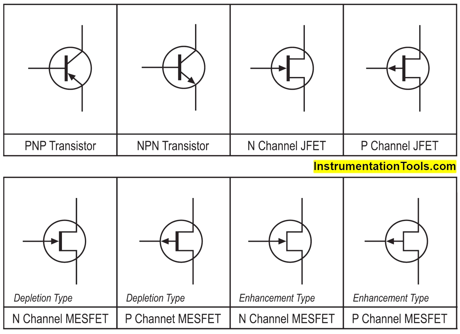
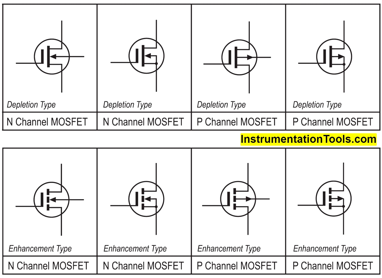
Fig 1 Symbols of FET and MOSFET
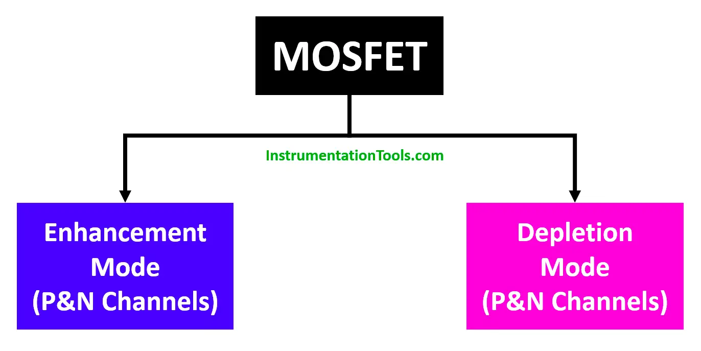
Fig 2 Types of MOSFET
Construction Details of Enhancement Mode Mosfet
Two heavily doped n+ source and the n+ drain region with heavy doping concentration are diffused on a lightly doped P-type substrate, spaced apart by about 25mm. Both a source and a drain will be formed by these N areas.
Over this surface, a thin layer of insulating SiO2 is formed. Holes are then cut into the oxide layer, through which aluminum contacts are produced for the source and drain. SiO2 is layered over the whole channel region, followed by an aluminum conducting layer that will serve as the Gate.
As opposed to depletion-type MOSFETs, enhancement-type N-channel MOSFETs are built differently since they lack a physical channel. It should be observed that the SiO2 layer is totally extended by the P-type substrate.
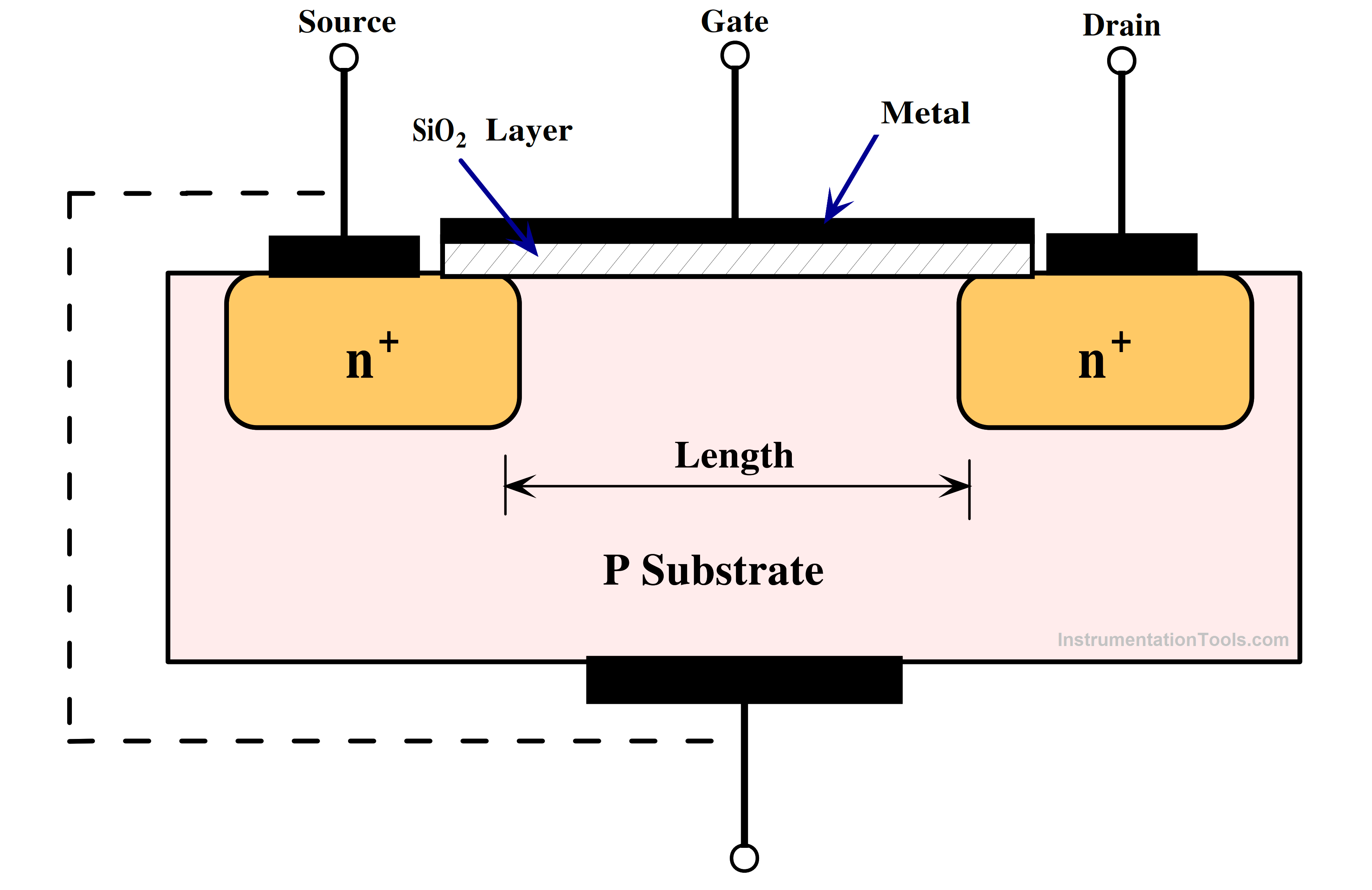
Fig 3 Enhancement Type MOSFET
Working of Enhancement MOSFET
The MOSFET’s current (i.e., drain to source current) is zero when the gate voltage (VGS 0) is open or zero. Due to one n+– p being reverse-biased, there is no current flowing through the load. An electric field is created close to the gate terminal when a positive voltage, such as VGS 0, is applied to the gate.
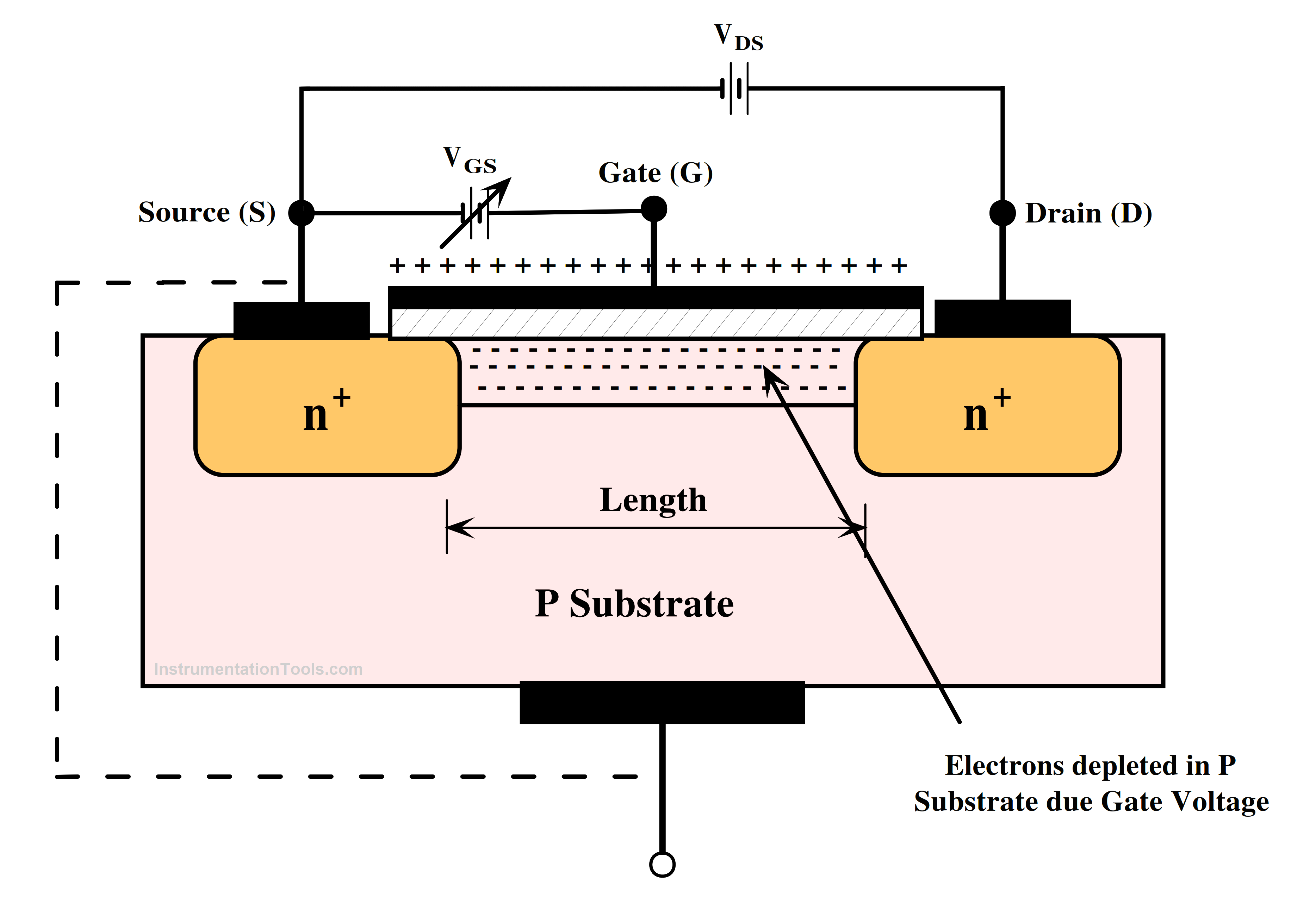
Fig 4 Biasing of Enhancement Type MOSFET
A layer of negative is created in a p-substrate area between two n+ layers as a result of capacitive action. SiO2 serves as a dielectric in the space between the layers of positive and negative charge. These negative charges create an n-channel, which allows current to flow.
The electron concentration in the n-channel increases with an increase in the gate’s positive voltage, increasing the current ID (Drain to Source). An enhancement kind of drain current is one where the gate voltage is increased.
Vi Characteristics of Power MOSFET
The Input/Transfer and Output Characteristics of the MOSFET are shown below
Input or Transfer Characteristics
The input Characteristics are drawn as Drain Current(ID) Versus Gate Source Voltage(VGS).
The minimal voltage necessary to initiate the flow of drain current is known as the threshold voltage, or VT. It ranges between 2 and 3 volts, which is the threshold voltage. When the Threshold voltage is Lesser than or equal to Gate Source Voltage the drain Current is zero or no flow of current in the load.
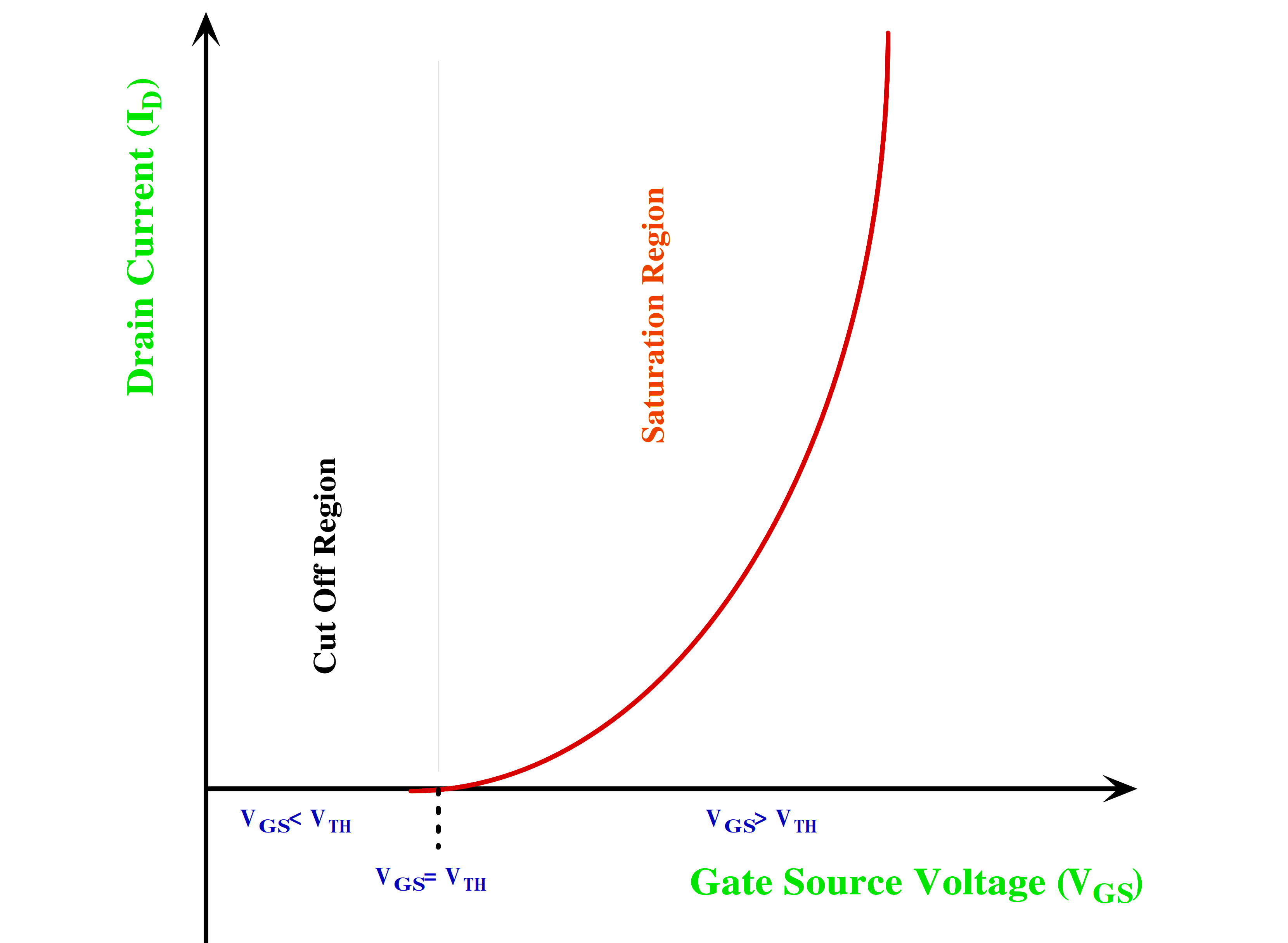
Fig 5 Input or Transfer Characteristics
After the Gate Source Voltage reaches the Threshold level the drain current starts to increase. The drain increases proportionately with an increase in the magnitude level of Gate Source Voltage. Since the device turns ON from the OFF stage to the ON stage the device is said to have transfer characteristics.
Output Characteristics
The output characteristics of the MOSFET have three regions
(a) Cut-off region (b) Ohmic or Linear region (c) Saturation region
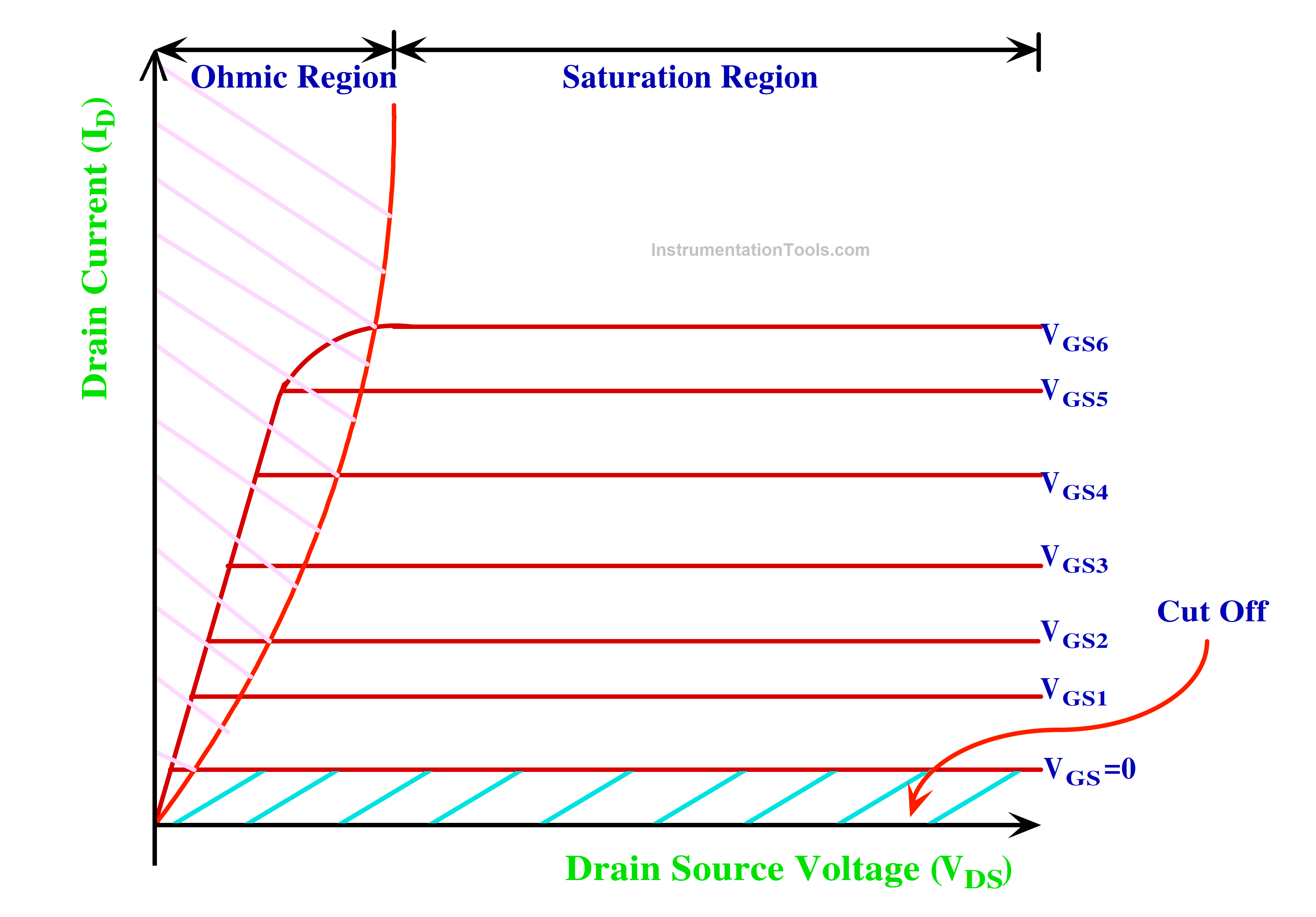
Fig 6 Output Characteristics
Cut-Off Region
The MOSFET will be OFF in the cut-off zone since there won’t be any current flowing through it. MOSFET is utilized when it is necessary for them to act as electronic switches since in this area they behave like an open switch.
Ohmic or Linear Region
The current IDS increases with a rise in the value of VDS in the ohmic or linear zone. It is possible to employ MOSFETs as amplifiers by configuring them to operate in this range.
Saturation Region
As soon as VDS rises over the pinch-off voltage VP, the MOSFETs enter the saturation area and their IDS remains constant. When this occurs, the device behaves as a closed switch through which an IDS value is saturated with information flows. As a result, anytime MOSFETs are needed to carry out switching operations, this operational area is picked.
The current through the device will be zero until the gate-to-source voltage (VGS) surpasses the threshold voltage (VT) in the transfer characteristics (drain-to-source current IDS against gate-to-source voltage VGS). This is because the channel that will connect the drain and source terminals is empty. The matching output characteristics (IDS vs VDS) show that even an increase in VDS will not cause current flow under this circumstance. This condition therefore only reflects the cut-off area of MOSFET functioning.
Once VGS crosses VT, the current through the device increases first with an increase in IDS (Ohmic region) and then saturates at a value as specified by the VGS (saturation area of operation). As a result, even the saturation current flowing through the device increases as VGS rises. Fig 6 makes this clear, showing that VGS3 > VGS2 > VGS1 and so on. Additionally, Fig 6. depicts the site of pinch-off voltage, from which it can be observed that VP rises as VGS rises.
Construction Details of Power MOSFET
Power MOSFETs have a vertical construction; the channel width determines the current rating while the doping and epitaxial layer thickness determine the voltage rating. They are useful for low-power switching applications because they can withstand high blocking voltage and high current.
High resistivity n– layer is epitaxially produced on an n+ substrate. The power MOSFET’s capacity to block voltage is determined by the thickness of the n–layer. The device’s primary structure is an n–type semiconductor that has been mildly doped. There are two strongly doped p–type areas in the body, spaced apart by L.
A thin coating of silicon dioxide (SiO2) that acts as a dielectric is now present on top of the substrate. This SiO2 dielectric layer is covered with an aluminum plate. The Source (S) terminal is positioned above the Drain (D) terminal in this arrangement, creating a vertical structure.
As a result, in VDMOS, a large number of n+ sources conducting in parallel allow the current to pass between the source and drain terminals vertically under the gate region. Because of this, the device’s ON state resistance, or RDS (ON), is substantially lower than it would be for a regular MOSFET, allowing it to take higher currents.
Working of Power MOSFET
When VDD is present and the gate circuit voltage is zero, the n– p junctions are reverse biased and there is no current flowing from the drain to the source.
When the gate terminal is turned positive in relation to the source, an electric field is created and, as is seen in Fig 7, electrons form an n– channel in the p regions.
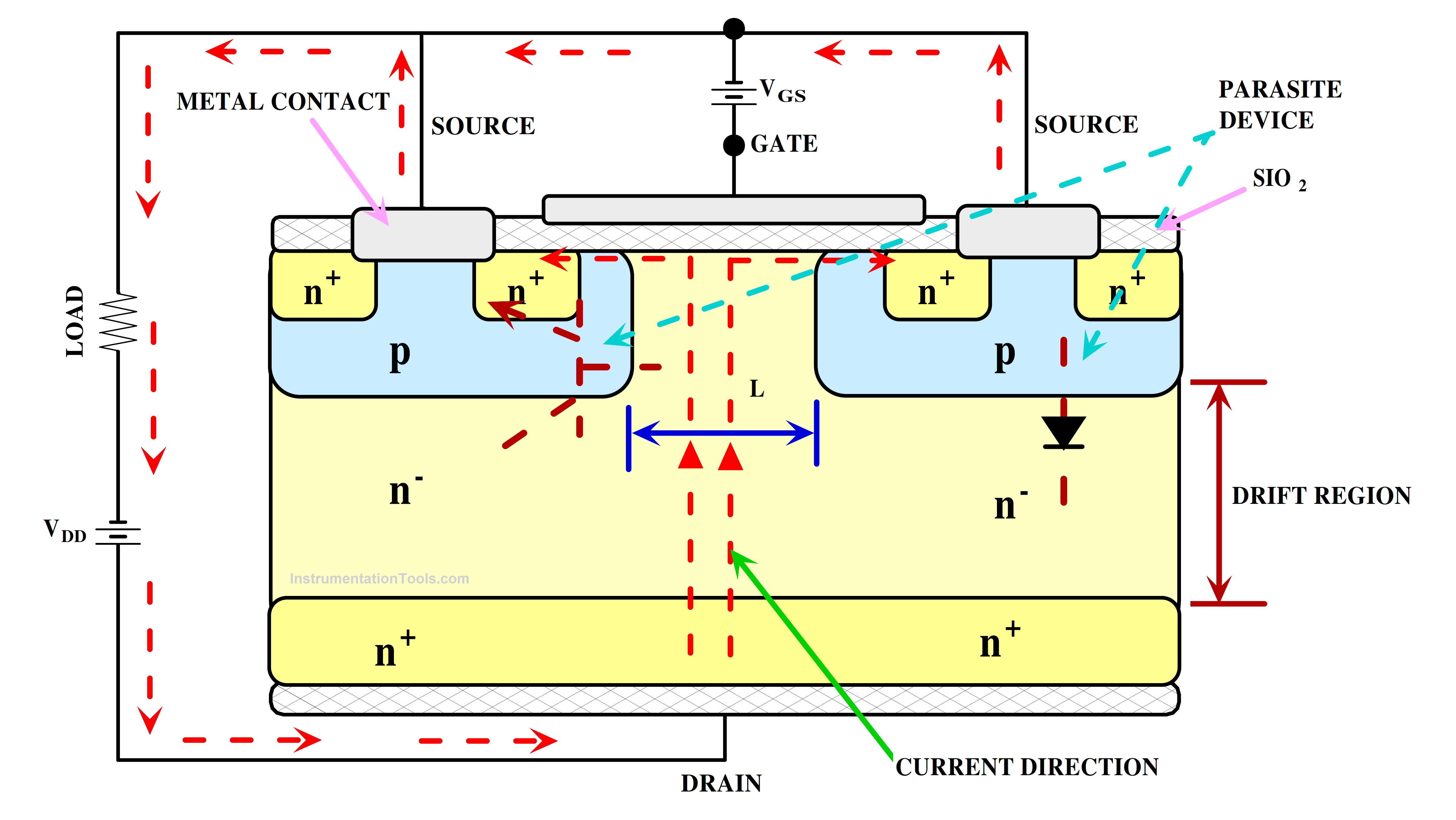
Fig 7 Power MOSFET Structure
As seen by the arrows, a current is therefore established from the drain to the source. Current ID increases as predicted when gate voltage rises. By using a small length for the channel, the length of the n-channel may be regulated, allowing the on resistance to be reduced.
Parasitic BJT & Diode
As seen in Fig 7, the construction of a power MOSFET includes a parasitic BJT. The base, emitter, and collector are the body area, source, and drain, respectively. Maintaining the base potential as near to the emitter potential as is practical will help keep this BJT off at all times. This is done by electrically shorting the MOSFET’s source and body.
If not, the device would enter the “latch up” condition and be destroyed by the potential at the base, which would activate the BJT and cause it to activate. A parasite p n diode is formed at the drain body of the MOSFET, as shown in Fig 7.
Switching Characteristics of Power MOSFET
The switching characteristics of a power MOSFET describe its behavior during the transition between the ON-state (conducting) and the OFF-state (non-conducting) when used in switching applications. Here’s a textual description of the switching characteristics:
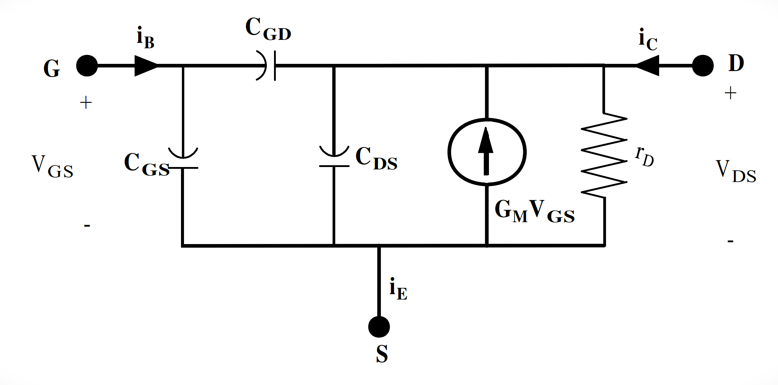
Fig 8 Small Signal Model of Mosfet
Turn-On (Switching from OFF to ON):
Delay Time (td): This is the time it takes for the MOSFET to start conducting significantly after a suitable gate voltage has been applied. It includes the time for the gate-source voltage to overcome any capacitances and turn on the MOSFET.
Rise Time (tr): The time taken for the drain current to rise from its initial OFF-state value to a specified percentage (usually 10% to 90%) of the final ON-state value.
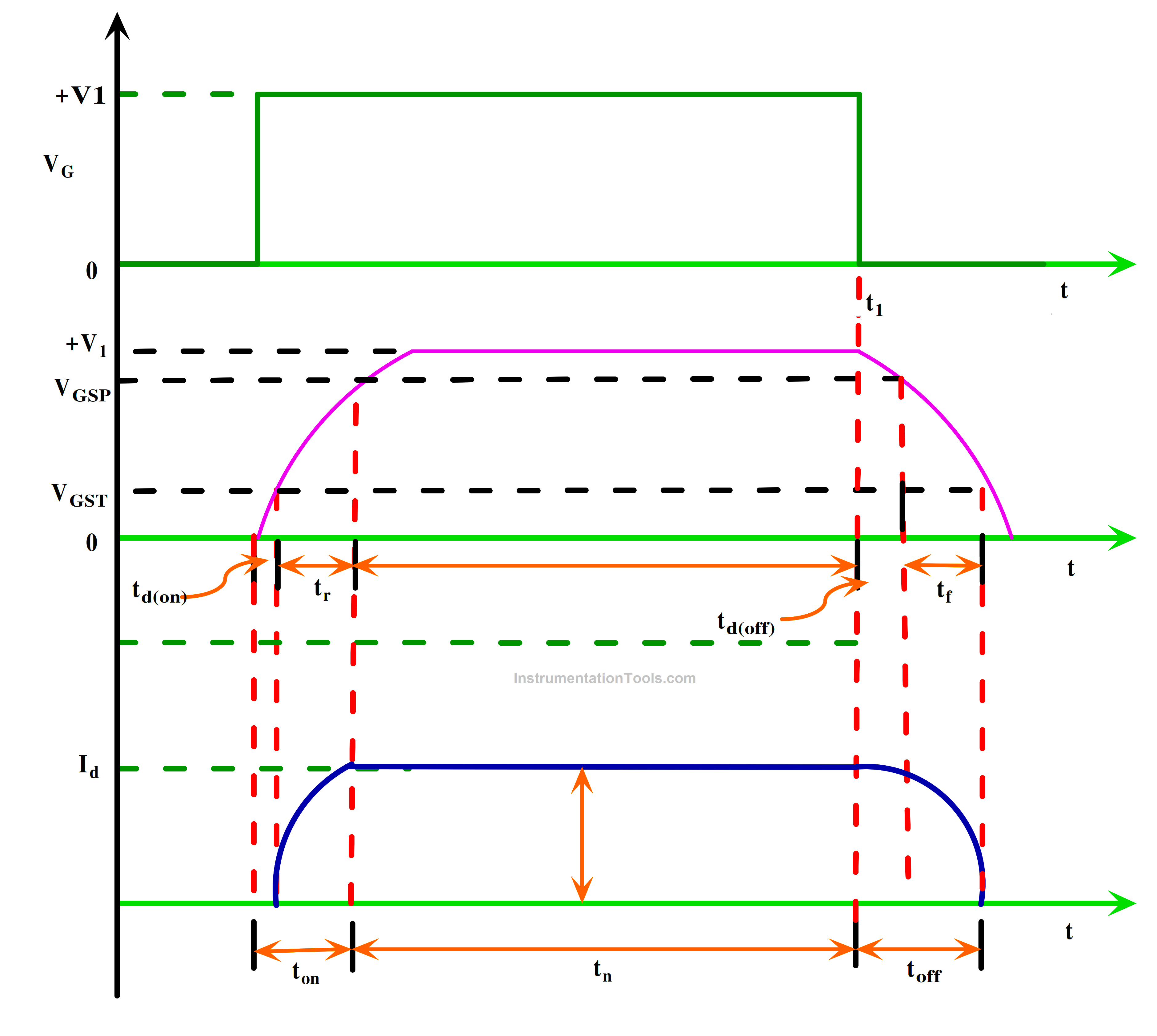
Fig 9 Switching Characteristics of Power MOSFET
Turn-Off (Switching from ON to OFF):
Fall Time (tf): The time taken for the drain current to fall from its initial ON-state value to a specified percentage (usually 90% to 10%) of the final OFF-state value.
Propagation Delay (tp): This is the time delay between the instant when the gate voltage is removed and the instant when the drain current has reduced to a specified level.
These characteristics are typically depicted in datasheets or application notes provided by the manufacturer. They are essential for designing and analyzing MOSFET switching circuits in power electronics applications. The actual shape and values of these characteristics depend on the specific MOSFET, its gate drive voltage, load conditions, and other circuit elements.
Advantages of Power MOSFET
- No Secondary Breakdown
- MOSFET is a Positive temperature coefficient device that results in good thermal stability.
- Used for high switching frequency
- Less on State resistance
- Higher switching speed
- No external circuit is required for commutation
Disadvantages of Power MOSFET
- Due to the non-symmetric nature of their blocking capability, MOSFETs can block high forward voltage instead of high reverse voltage.
- The device may be damaged by a constant current
- Since the on-state voltage is so high. Consequently, there is a large loss of on-state power.
Applications of Power MOSFET
- High frequency-based inverter
- Display driver
- Motor control
- Relay control
- and much more….
If you liked this article, then please subscribe to our YouTube Channel for Instrumentation, Electrical, PLC, and SCADA video tutorials.
You can also follow us on Facebook and Twitter to receive daily updates.
Read Next:
- What is Power Electronics?
- SCR Switching Characteristics
- Types of Power Electronic Devices
- Power Diode Characteristics
- Power Transistor Structure & Biasing