Thyristor-triggering circuits are electronic circuits used to control the firing or triggering of thyristors (SCR). Thyristors are semiconductor devices that can be turned on by applying a gate current and remain on until the main current flowing through them drops below a certain threshold.
These triggering circuits are essential in various applications, including motor control, power supplies, lighting control, and voltage regulation.
Types of Thyristor Triggering Circuits
There are several methods to trigger thyristors, and the choice of triggering circuit depends on the specific requirements of the application.
Here are some common thyristors triggering circuits:
Resistance Triggering Circuit
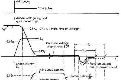
Thyristors can be activated by a step-down DC voltage, a slow-rising DC signal, or a rectified positive half-wave signal.
Triggering occurs when the gate terminal’s applied voltage is higher than the VGT level.
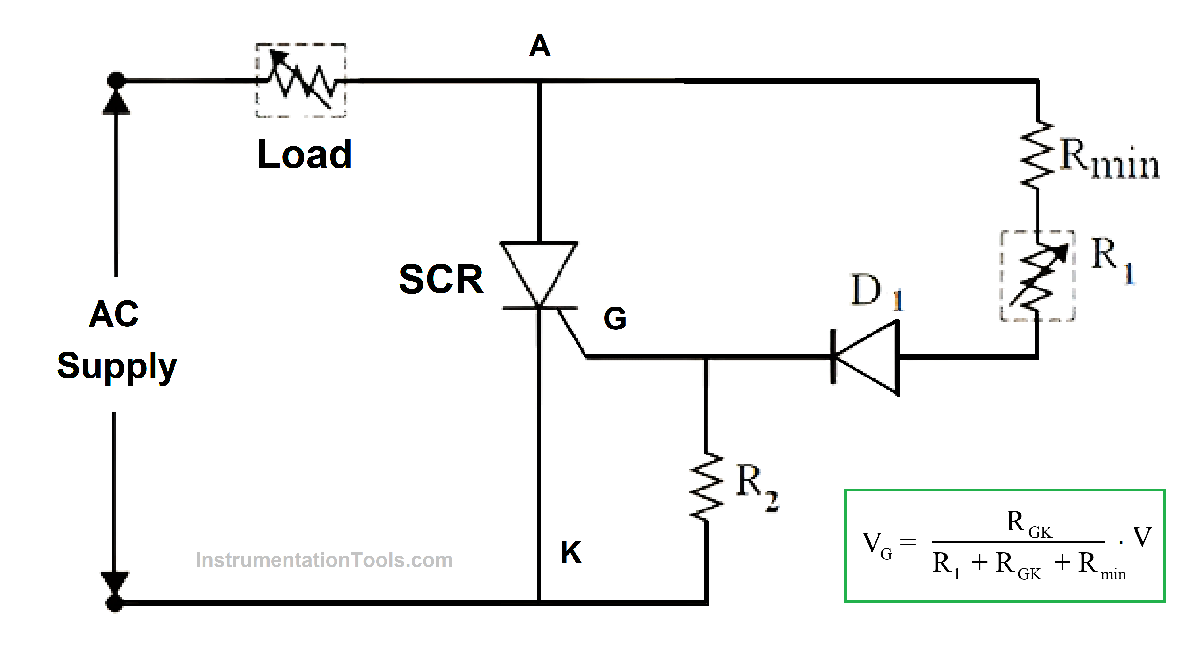
Fig 1. Resistance Triggering Circuit
An AC circuit’s trigger circuit and waveforms are shown in Fig. 1.
The input supply voltage (V) appears across the SCR prior to the SCR conducting. R2 (which is big compared to Gate to Cathode Resistance, RGK) and the voltage drop across D1 are ignored, and the gate voltage is provided by the equation (shown in the above image).
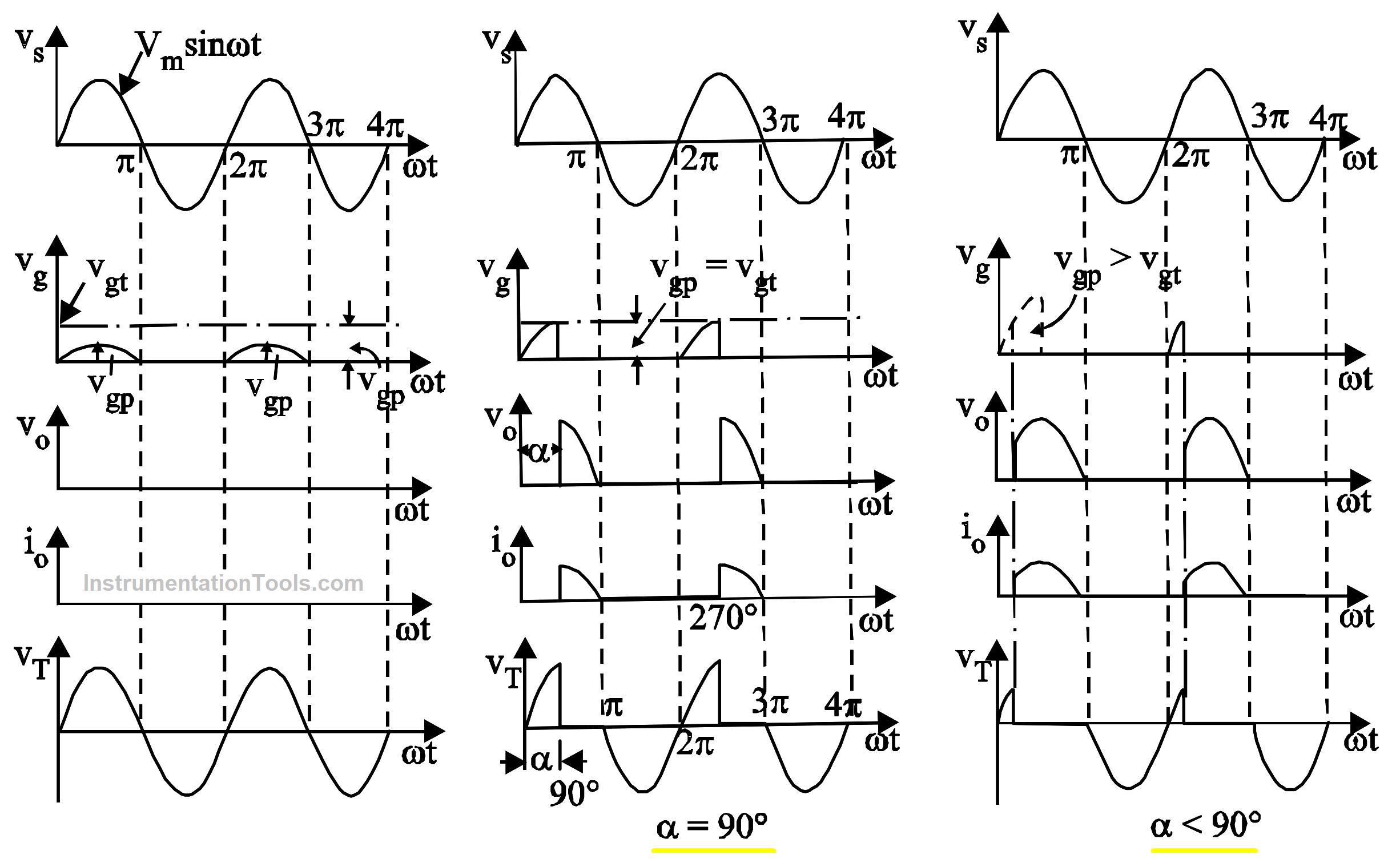
Fig 2. Resistance firing of an SCR in a half-wave circuit with DC load
(a) No triggering of SCR (Left) (b) α = 90° (Center) (c) α < 90° (left)
Where the supply voltage V = Vmsint and the forward gate-to-cathode resistance is RGK. Conduction of the SCR starts as soon as VG hits the VGT level and produces the necessary gate current. Voltage VAK decreases. As a result, VG likewise decreases to practically zero and v appears throughout the load.
Now, by increasing R1, we can raise by decreasing VR2 and VR1. The curve 3 demonstrates that with a larger R1, the circuit eventually fails to activate the gadget. In this case, curve 2 of V0 in the Fig. 2 shows that the control is only effective at 90°. In the same way, IG shouldn’t go above IGM. As a result, the resistor’s Rmin value can be calculated using
( Vm / Rmin ) ≤ IGM
A resistor R2 placed between the G and K terminals of the SCR improves this circuit much further. So, in the worst-case scenario, the voltage across R2 shouldn’t be higher than the VGM level. In light of this, the resistor’s R2 maximum value is given by
[ R2 / (R2 + Rmin)] Vm ≤ VGM
Resistor-Capacitor (RC) Triggering Circuit
When the capacitor charges through a resistor, it eventually reaches a voltage level that triggers the thyristor gate. The thyristors are activated by an RC network, which also generates a phase-shifted signal in an AC circuit and a slow-rising signal in a DC circuit. The range of α can be expanded past in several situations.
An RC circuit’s trigger circuit is shown in Fig. 3. Across the RC branch, the supply voltage may be seen. A linear RC circuit’s sinusoidal steady-state response can be used to examine the circuit while ignoring the discharge of the capacitor during the thyristor’s conduction period. Thus, it is possible to alter the phase angle of the capacitor voltage, which ranges from 0° to practically 90°.
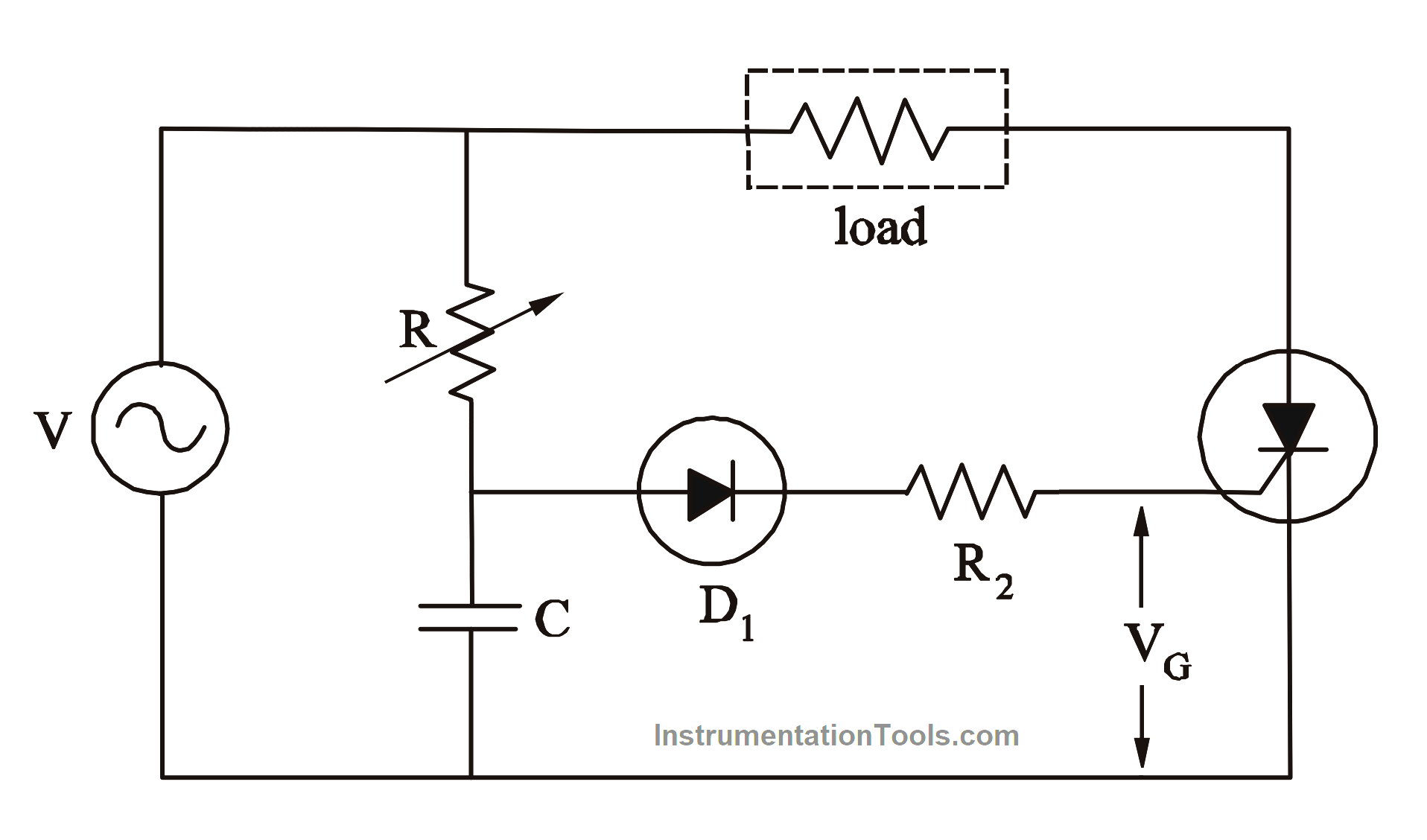
Fig 3. RC trigger circuits
The capacitor voltage’s (Vc) rms value, which is equal to Vcosθ, will, however, substantially fall the greater the value of θ. Thyristor conduction occurs when Vc exceeds VGT in the positive half-cycle. This makes it possible to control the RC firing circuit over a large range (beyond 90°). R, phase angle (θ), and Vc change in magnitude are all variables.
Additionally, the gate-current limiting resistor R2 (like resistance-trigger circuits) can be used to control the magnitude. When the RC branch is connected across the SCR, the circuit layout can be improved.
The voltage across the RC branch similarly drops to a very low level (preferably zero) when the SCR is conducted. As a result, there is a considerable decrease in the gate circuit’s power dissipation.
Half Wave Triggering Circuit
This circuit has been made possible by adding a second diode (D2) to the one in Fig. 4. The charging process begins at the point of negative zero crossover and continues until the negative peak of V, (- Ö2 V).
The voltage at the cathode (v) and the voltage at the anode of D2 are then equal.
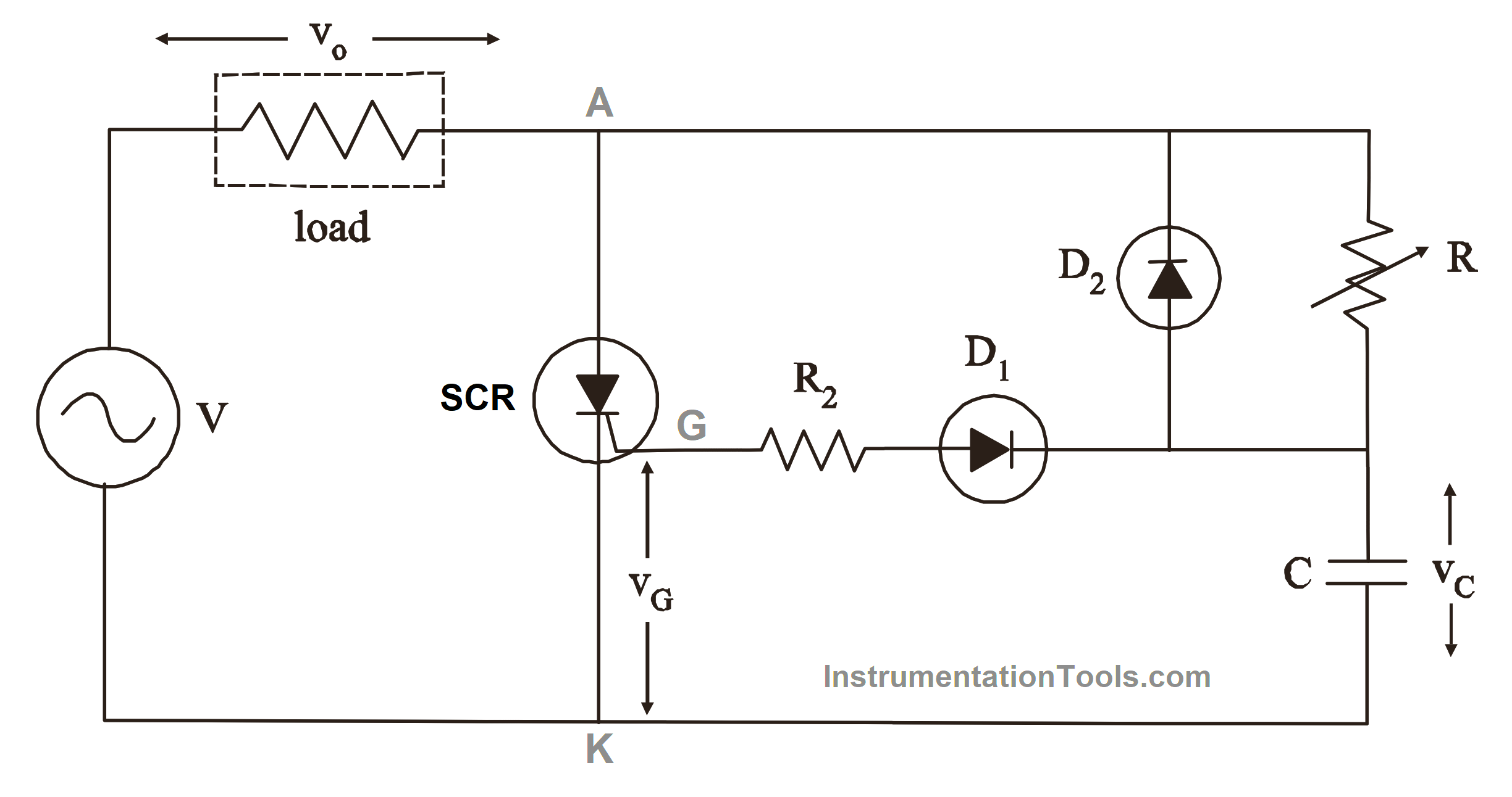
Fig 4. Half Wave RC trigger circuits
As a result, D2 experiences a drop in current and adopts a reverse bias. Currently, R is used to charge the capacitor, and the time period RC determines the charging rate.
Conduction of the SCR occurs when vG (rectified vc) slightly exceeds VGT.
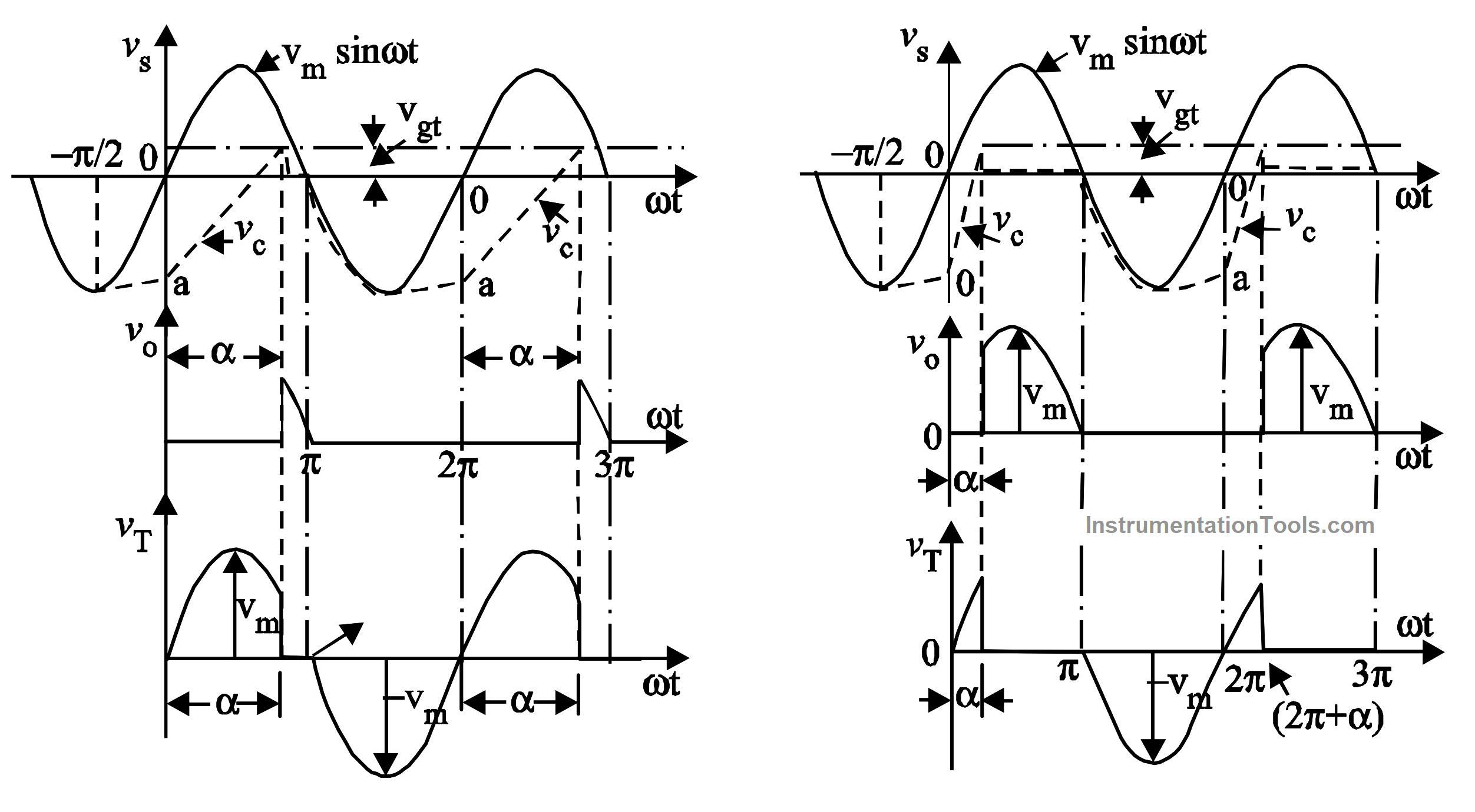
Fig 5. Half Wave RC trigger circuits Waveform
Full Wave Triggering Circuit
By integrating a diode bridge into the prior circuit, this circuit has been made possible. According to Fig.6. a capacitor is charged through R, and the charging rate is determined by RC (duration).
Conduction of SCR occurs when VG (rectified VC) slightly exceeds VGT. The charging rate of the capacitor is thus variable simply by changing R.
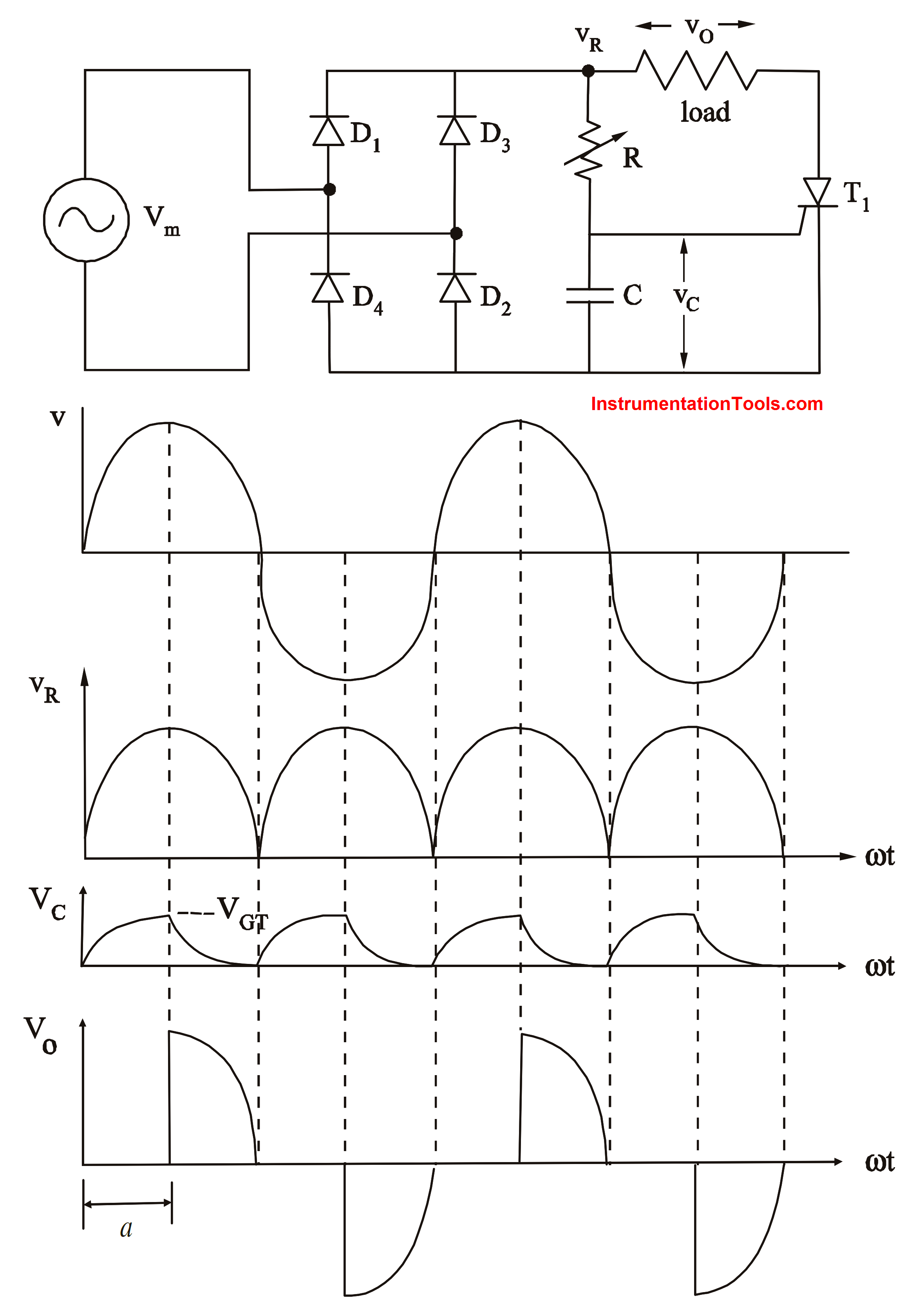
Fig. 6 A full wave RC trigger circuit
The capacitor in this circuit begins to charge at each zero-crossover instant, and up until the thyristor is triggered, it only receives a half-wave rectified voltage. The whole response of an RC circuit to a sinusoidal (half-wave) stimulus can be used to examine the circuit.
UJT (Unijunction Transistor) Triggering Circuit
UJT is a three-layer, two-terminal device that generates a trigger pulse when biased properly. It is commonly used for triggering SCRs. When the UJT fires, it provides a pulse to the gate of the thyristor, turning it on.
The capacitor C1 begins charging through R1 as soon as the circuit is energized by DC. The UJT turns ON when the voltage across the capacitor reaches peak point voltage.
The SCR is turned on after the UJT is turned on because the SCR’s gate receives the pulse sent by the RG. Through the SCR, the load current passes. R2 and B2 of the UJT discharge the capacitor C1 during this process.
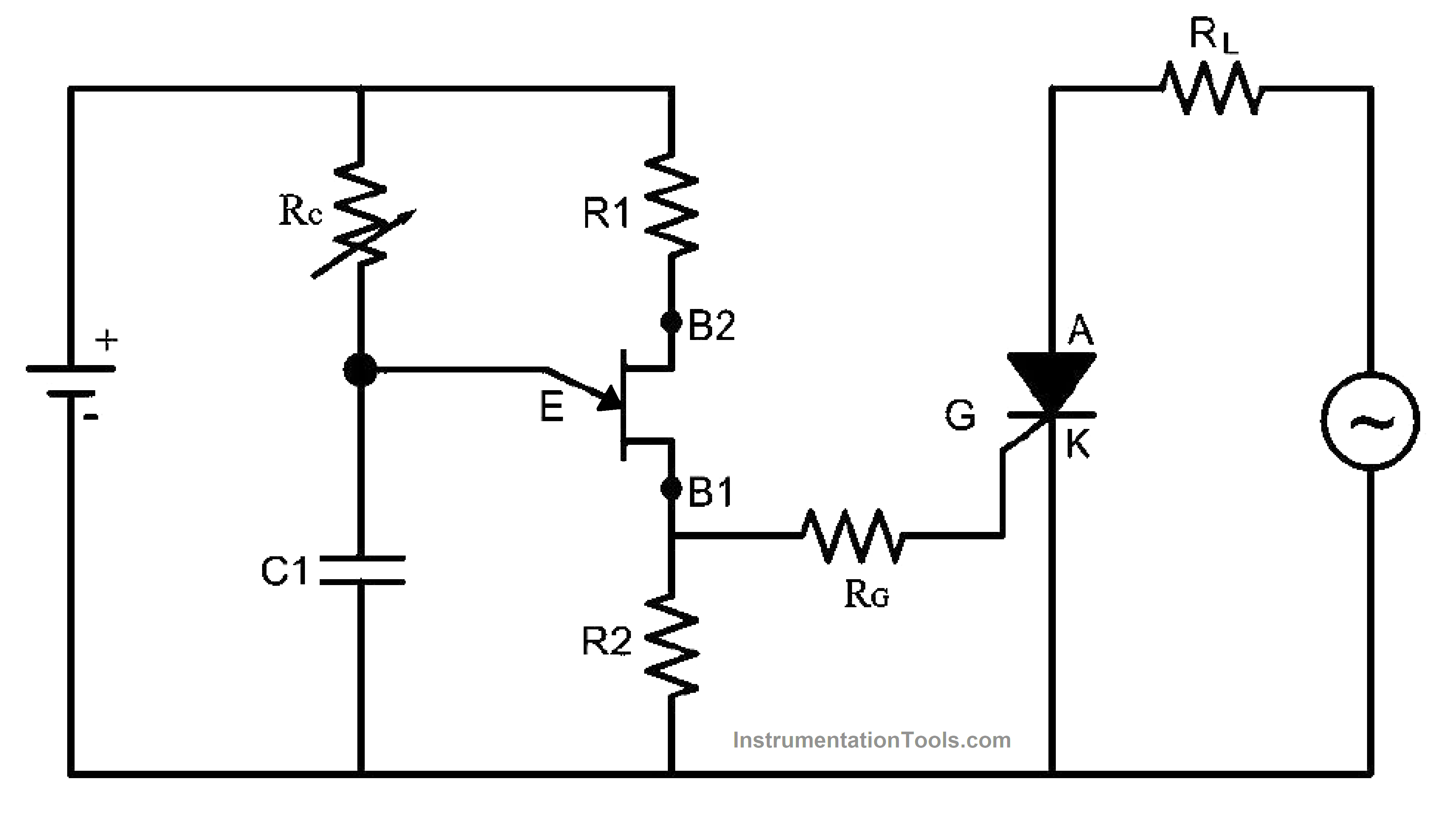
Fig. 7 UJT Firing circuit
The UJT switches off and the capacitor begins to charge once more when the voltage across the capacitor reaches 2.0 V. As R1’s resistance rises, the capacitor’s rate of charging drops.
As a result, the firing angle will increase and the load current will decrease. Because the UJT is supplied by a DC supply while the SCR is energized by an AC supply, there is no synchronism, and the firing angle changes in value during each positive half cycle.
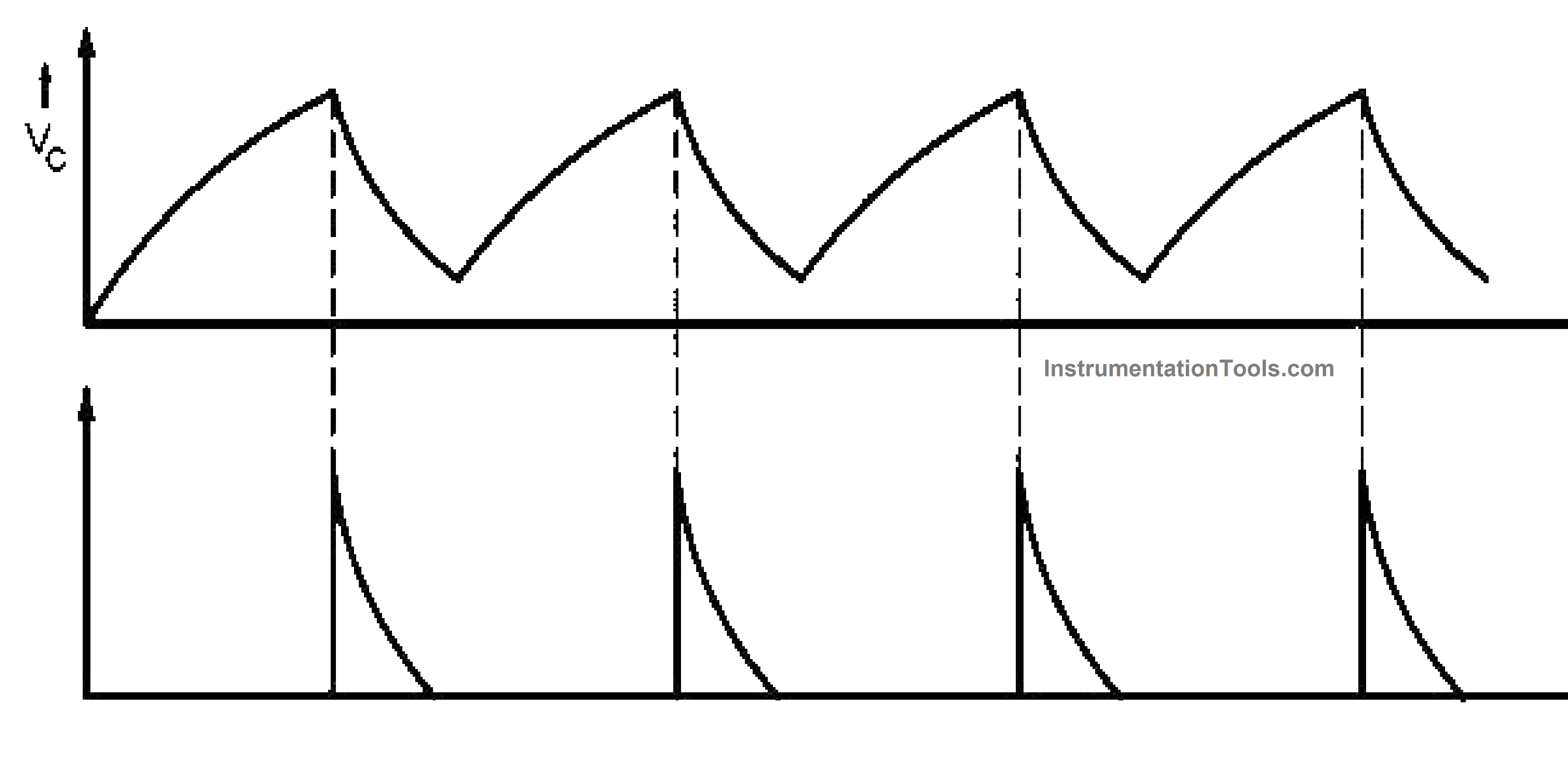
Fig. 8 Firing pulse of UJT for SCR
The UJT receives DC power from the same sources during the positive half cycle in order to maintain the same firing angle. Supply to the load only occurs during half of the cycle.
DIAC-SCR/TRIAC Triggering Circuit
In this circuit, a DIAC (Diode for Alternating Current) is used to trigger a SCR/TRIAC (Triode for Alternating Current). The DIAC provides a voltage pulse to the SCR/TRIAC gate, which in turn controls the main thyristor.
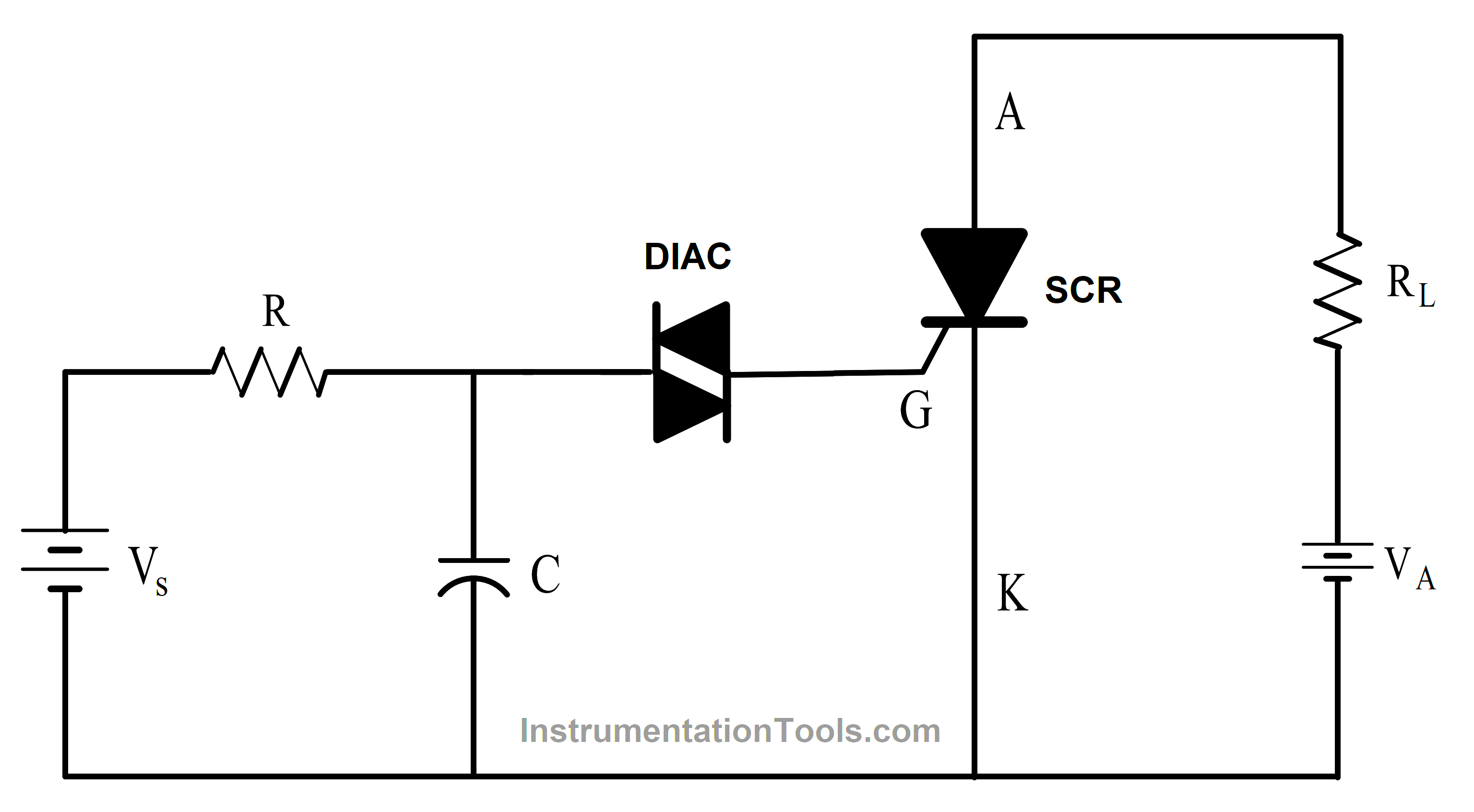
Fig. 9 DIAC Firing circuit
A capacitor is progressively charged in a similar circuit employing a DIAC over time equal to the RC time constant.
The DIAC is switched into conduction once the capacitor has been charged to a voltage equal to the DIAC’s breakover voltage.
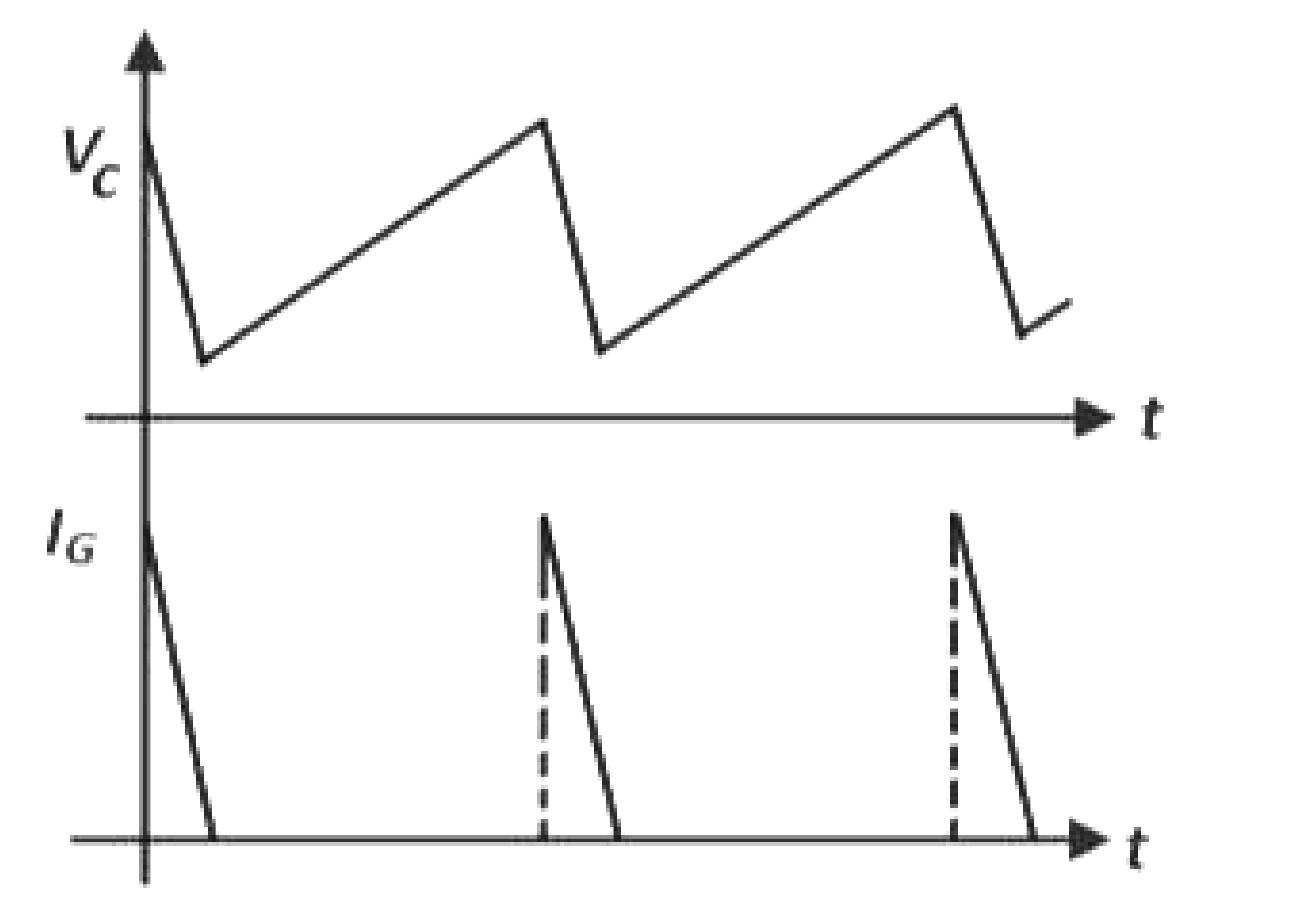
Fig. 10 Firing pulse of DIAC for SCR
Next, a quick discharge of the capacitor occurs into the SCR’s gate terminal. The cycle is repeated after a brief time, at which point the DIAC shuts off.
With this setup, the capacitor is charged from a DC source using relatively little power, but a substantial amount of power is provided for a brief period of time, ensuring a dependable SCR turn-on.
Pulse Transformer Triggering Circuit
A pulse transformer is used to provide an isolated and controlled pulse to the thyristor gate. It can be used when electrical isolation between the control circuit and the power circuit is necessary.
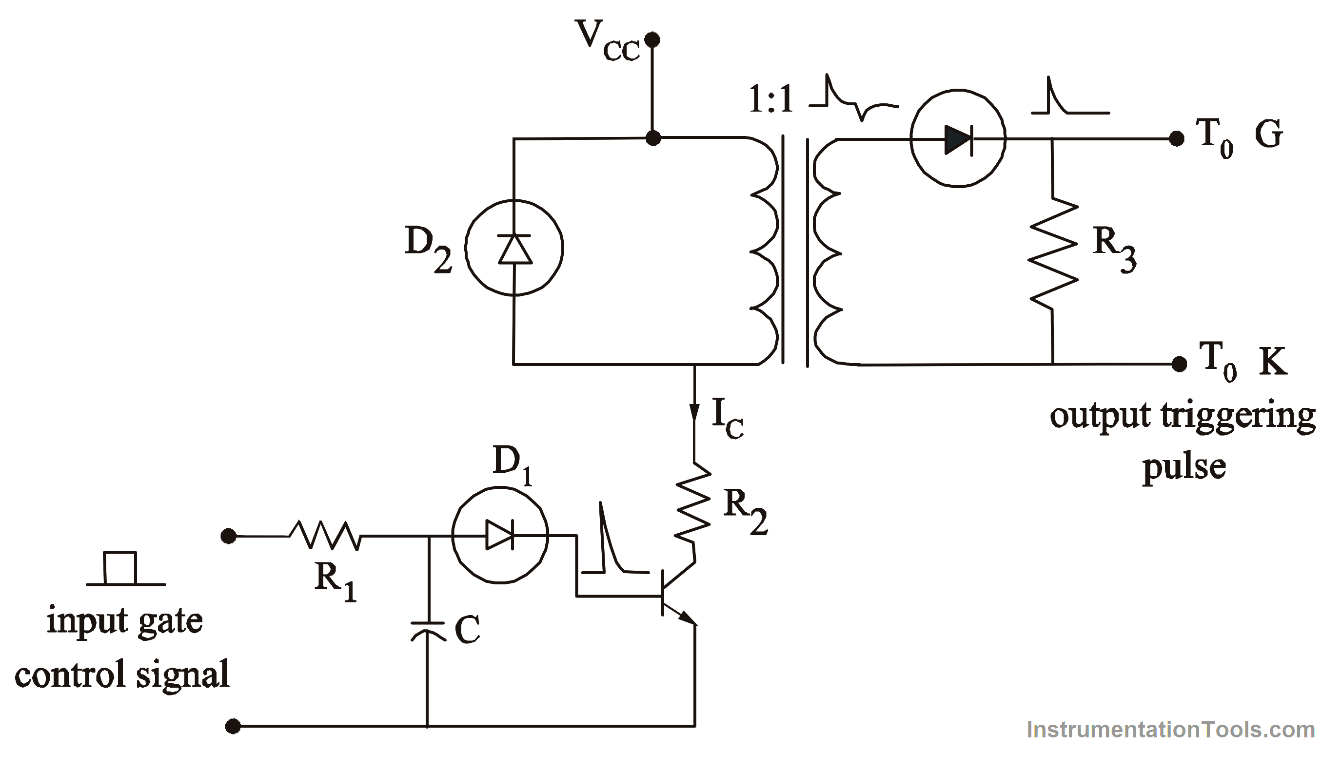
Fig. 11 Pulse transformer-based Firing Scheme
A step input signal is transformed into sharp positive and negative pulses by a differentiator circuit, R1 C, as shown in Fig.11 Amplification of the positive pulse by the transistor.
The input is isolated using a pulse transformer, and a thyristor’s gate and cathode terminals are connected using a diode (D3) that only permits the positive half of the amplified signal. D2 offers the pulse transformer’s primary winding’s inductive current a free-flowing channel.
This safeguards the transistor from large voltage spikes that might be produced as a result of the transistor being turned off, which would cause the inductive current Ldi/dt to abruptly cease. Following a certain interval, the anode current of a thyristor reaches the latching current level. Consequently, a long pulse is necessary for a successful trigger on an inductive load.
To achieve this, R2 and a capacitor are linked in parallel. The pulse duration is limited to 50µs to 100µs, though, to prevent saturation of the pulse transformer’s core from stretched unidirectional current.
In converter circuits with inductive loads, a constant gate signal is necessary, however doing so raises thyristor losses and lowers voltage withstand or blocking capabilities. An alternative is to supply a train of high-frequency trigger pulses during the whole conduction period.
Opto Isolator Triggering Circuit
Opto isolators (also known as optocouplers) use an LED and a photodetector to provide electrical isolation. The LED is driven by a control circuit, and the photodetector’s output triggers the thyristor gate.
On a single IC chip, an infrared light-emitting diode and a photo-SCR are manufactured. The input gate control signal conducts and emits light to put the photo-SCR into conduction mode when it receives a pulse.
As a result, the primary SCR is switched. Great electronic components called optocouplers and opto-isolators make it possible to operate components like power transistors and triacs using a controller board, a digital switch, or a low-voltage data signal from a logic gate.
Opto-couplers’ primary benefit is their excellent electrical isolation between the input and output terminals, which enables relatively small digital signals to regulate considerably greater AC voltages, currents, and power with only a small amount of signal.
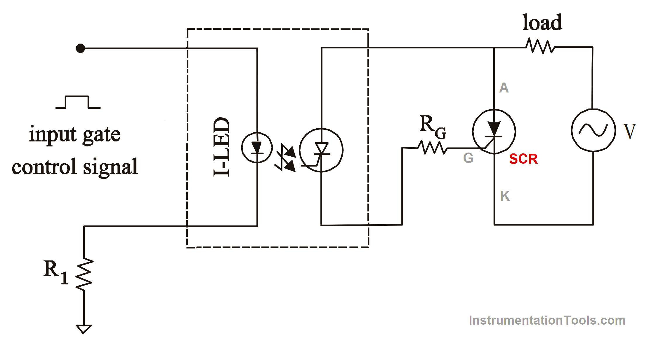
Fig. 12 Opto Coupler Firing Circuit
Optocouplers using an SCR (thyristor) or triac as the photo-detecting device are primarily developed for AC power-control applications, though they can be utilized with both DC and AC signals. The primary benefit of photo-SCRs and photo-triacs is complete isolation from any noise or voltage spikes present on the AC power supply line.
Additionally, zero-crossing detection of the sinusoidal waveform reduces switching and inrush currents, protecting any power semiconductors used from thermal stress and shock.
Microcontroller or Digital Logic-Based Triggering
In modern applications, microcontrollers or digital logic circuits are often used to generate precise trigger signals. They offer flexibility and programmability, making them suitable for advanced control systems.
The choice of triggering circuit depends on factors like the required firing angle, voltage and current ratings, isolation requirements, and the specific application. Some circuits are more suitable for phase control, while others are better for on/off switching. It’s essential to design and select the appropriate triggering circuit to meet the desired performance and safety requirements of the thyristor-based system.
Synchronizing the microcontroller with the AC input voltage is required in a Microcontroller Firing Circuit of a Thyristor. Zero-crossing detectors are required for this purpose. The power circuit and control circuit are isolated using a potential transformer, which also lowers the AC supply voltage to 5 V AC.
The microcontroller detects the zero-crossing at the rising edge of the AC voltage waveform by reading the output from the zero-crossing detector through an input port. The microprocessor then runs a time delay loop, generates the trigger or firing pulse, and holds it for brief periods of time.
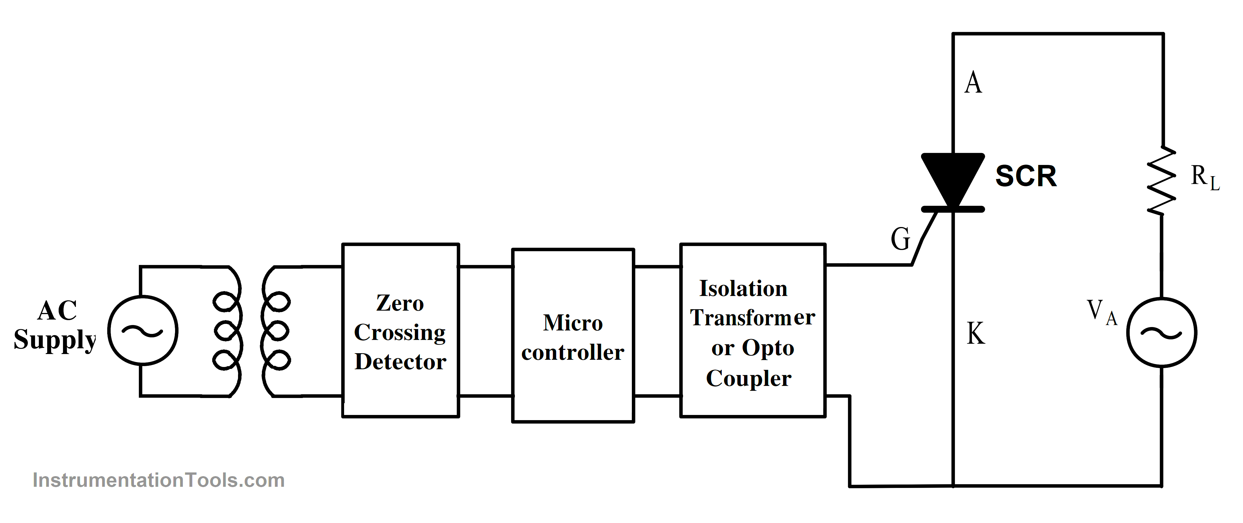
Fig. 13 Microcontroller Triggering Circuit
The output trigger or firing pulse cannot be utilized to directly trigger the thyristor due to its low power capacity. The output of the opto-coupler is applied to the gate-cathode terminals of the thyristor, and an opto-isolator circuit has been linked to the microcontroller output port as a result.
When the gate pulse is applied and the thyristor is forward-biased, the thyristor turns on and current flows through the load. Fig. 13 displays the AC input voltage, output of the zero crossing detector, firing pulse, and output voltage waveform for a delay angle.
When the AC waveform crosses zero, the microcontroller once more analyses the output of the zero-crossing detector to identify the subsequent rising edge. The microcontroller then creates the subsequent trigger pulse after the time delay. In consideration of this, the aforementioned process will be carried out repeatedly in a cycle.
Reference
- “Power Electronics” P. S. Bimbhra, Khanna Publishers, 2012
- “Power Electronics: Circuits, Devices and Applications”, M H Rashid, Pearson Education
- “Power Electronics”, M-Scheme, K.V. Kandasamy, 2020.
If you liked this article, then please subscribe to our YouTube Channel for Instrumentation, Electrical, PLC, and SCADA video tutorials.
You can also follow us on Facebook and Twitter to receive daily updates.