A power diode is a type of diode that is often used in power electronics circuits. A power diode, like a standard diode, is the diode symbol shown in Fig 1. It has two terminals and conducts electricity in just one direction.
Power Diode
A power diode is built differently than a conventional diode to allow for this increased current rating. To improve its power handling capability, the power diode’s structure is modified slightly from a simple p-n junction diode.
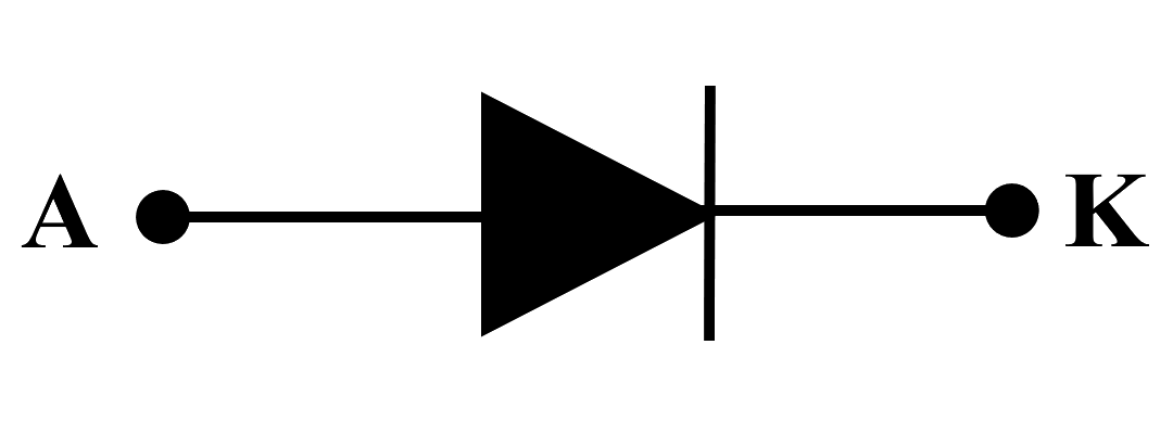
Fig 1 Diode Symbol
A diode operates as a switch to accomplish a variety of activities, including switching in rectifiers, freewheeling in switching regulators, charge revision of capacitors and energy transmission between components, trapped energy recovery, voltage isolation, and energy feedback from the load to the power source.
Diode as a Switch
It is a two-terminal device, with terminal A serving as the anode and terminal K serving as the cathode. If terminal A has a greater potential than terminal K, the device is said to be forward-biased, and a current known as forward current (IF) flows through the device in the direction seen in Fig 2. This results in a negligible voltage drop (of around 1V) across the device, which under ideal circumstances is often neglected.
On the other hand, when a diode is reverse biased, it does not conduct and a real diode does experience a little current flowing in the opposite direction termed the leakage current. In a perfect diode, the leakage current and the forward voltage drop are both neglected. A diode is typically regarded as the best static switch for power electronics applications.
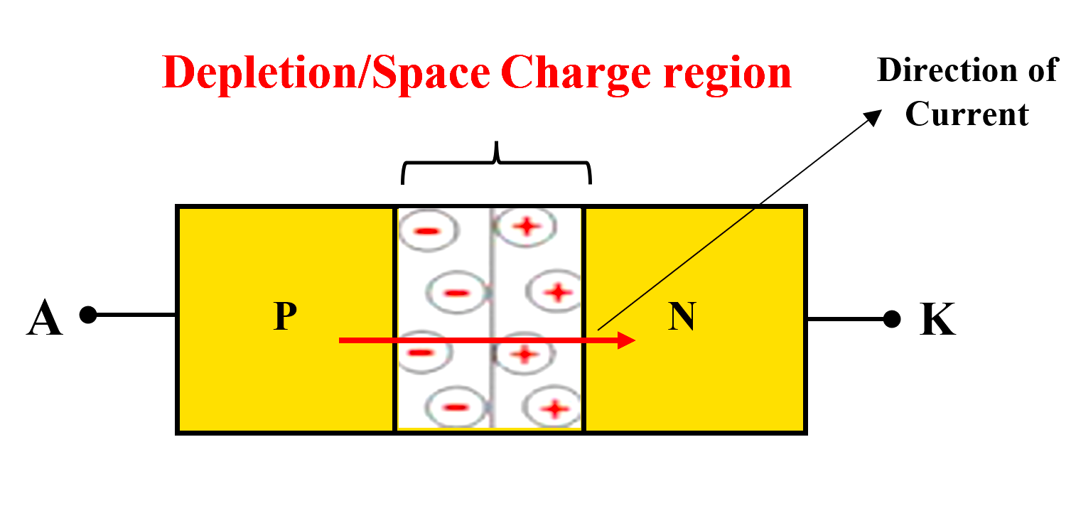
Fig 2 The general structure of the PN junction diode
DC Diode Parameters
Forward voltage, VF: When a diode is forward biased, forward voltage, or VF, is the voltage drop across A and K at a specific current level.
Breakdown voltage, VB: The breakdown voltage(VB), is the voltage drop across the diode when its reverse biased.
Reverse current IR: Reversed current IR is the current at a certain voltage that is lower than the breakdown voltage.
Drift Region(Only in Power Diode): The n– region acts as a drift region. The n– region sums up the diode’s ohmic resistance in forward conduction mode, which results in significant power dissipation.
Characteristics of Diode
The characteristics of an ideal diode deviate from the ideals of zero forward and infinite reverse impedance, as seen in Fig. 3.1 A voltage drop occurs in the forward direction due to a potential barrier brought on by the distribution of charges close to the junction and other factors.
For currents in the usual range, this is in the region of 1V for silicon. In the opposite direction, a very small current that is essentially independent of the voltage flows within the typical working range of voltage. For practical purposes, Fig. 3.2 frequently serves as a representation of the static features.
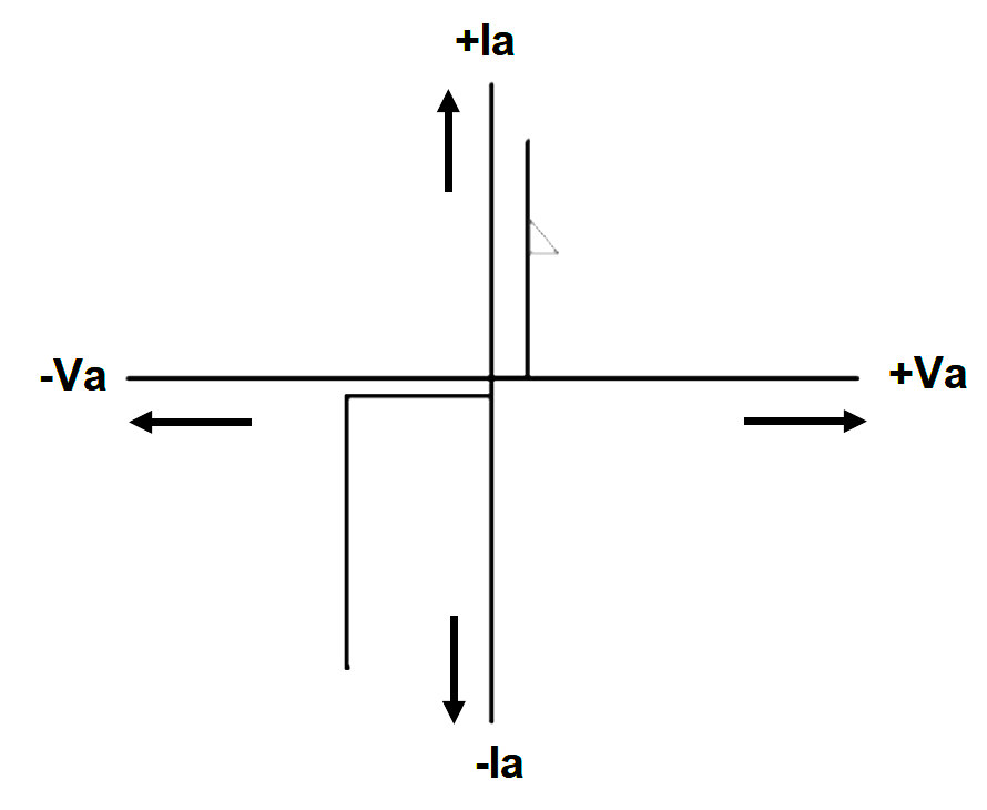
Fig 3.1 Ideal diode VI Characteristics
A threshold voltage Vo and a linear incremental or slope resistance, r, are used to represent the forward characteristic in Fig. 3. Regardless of voltage within the usual operating range, the reverse characteristic is constant throughout the whole range of potential leakage currents.
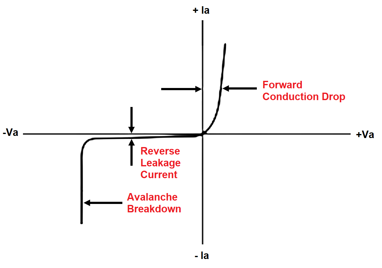
Fig 3.2 Practical Diode VI Characteristics
Construction of Power Diode
An n+ strongly doped substrate is taken into consideration, over which an n- layer is developed epitaxially. Diffusion of the p+ layer also occurs over the n- area. While the n+ substrate serves as the cathode connection, this p+ area serves as the anode connection. The simple structure of the Power diode is shown in Fig 4.
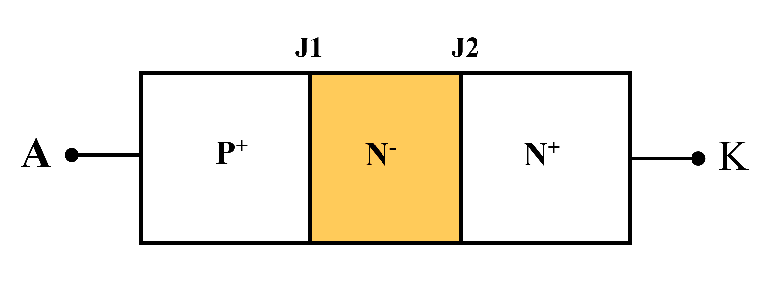
Fig 4 Simple Structure of Power Diode
We were able to see while studying the p-n junction diode that no such structure was present there. Thus, the p+ and n+ areas serve as the anode and cathode, respectively, while the n- region serves as the drift region. The depletion zone is absorbed inside the drift region in the reverse-biased state.
The breakdown voltage of the diode when reverse biased exhibits a direct correlation with the thickness of the n-region. Therefore, the breakdown voltage will be higher the broader the n- region.
Working of Power Diode
In that instance, junction J1 becomes forward-biased and the majority of carriers (holes) from the p+ area begin to inject into the n– drift region. The holes in the p+ area will recombine with the electrons in the n– region when the injection rate is low.
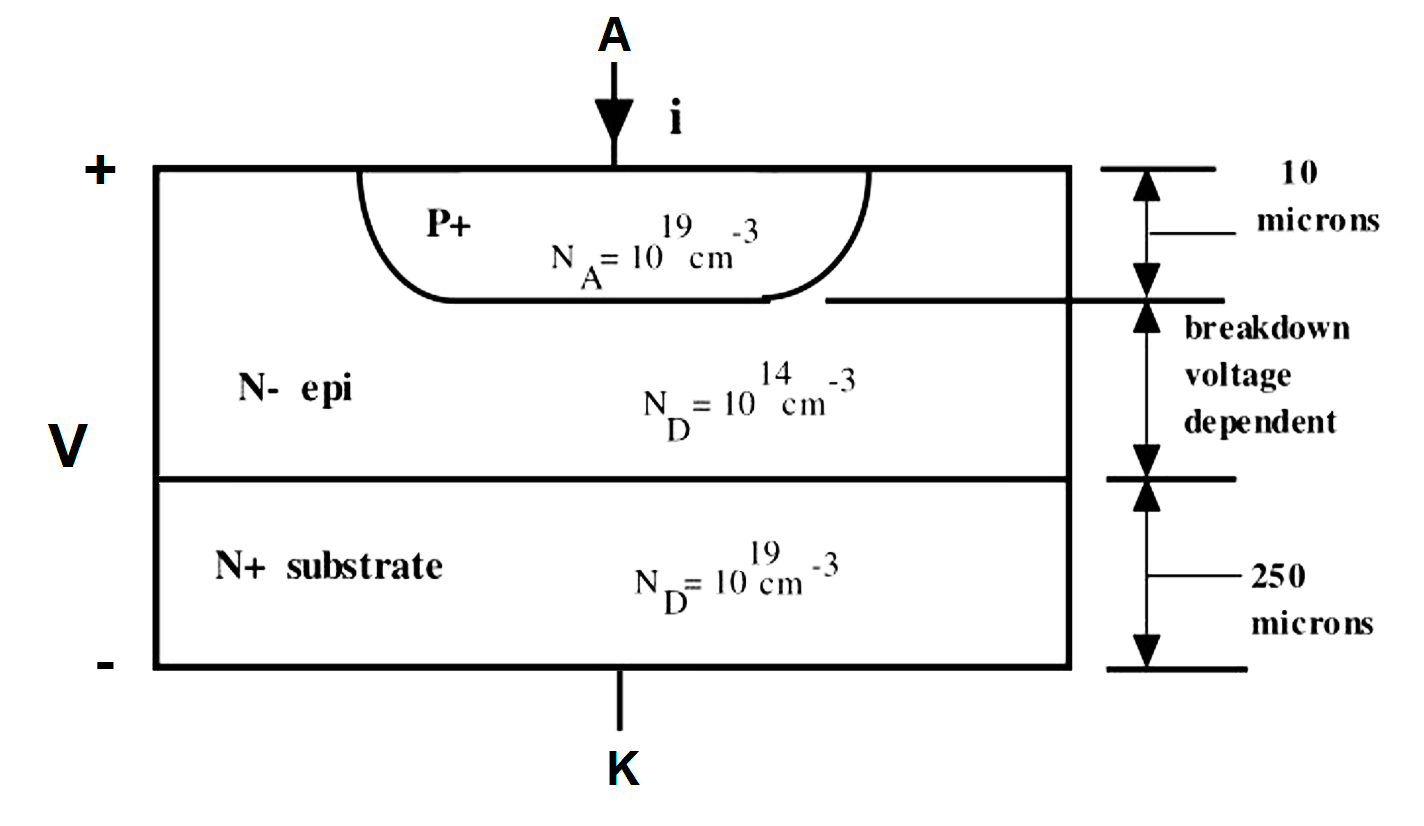
Fig 5 Layer Diagram of Power Diode
However, if the rate of injection is raised, holes will enter and rejoin at the junction J2, the n+ region’s electrons. This term is called Double injection. Once the threshold is reached, the diode begins conducting significantly because of this inflow of carriers and recombination inside the drift area.
Fig 6 Actual Power Diode
Diode Reverse Recovery Characteristics
Due to accumulated charges in the two layers, the forward diode current decays to zero yet the diode continues to operate in the reverse direction. For a period of time known as the reverse recovery time (trr), the reverse current flows. Restoration of the diode’s blocking until the reverse recovery current reaches a steady state.
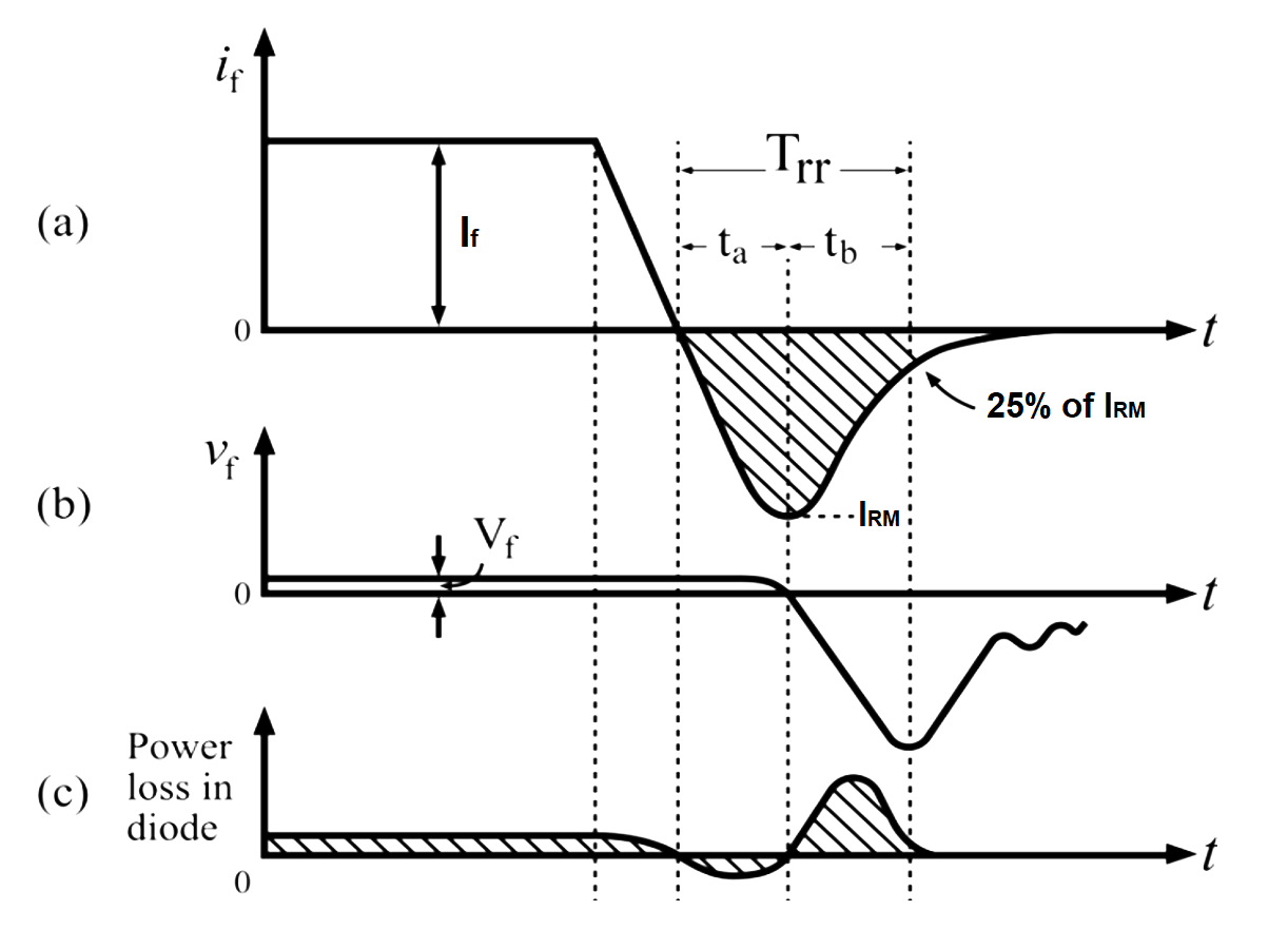
Fig 7 Dynamic Characteristics of Power Diode. (a) Forward Current during ON to OFF (b) Forward Voltage during ON to OFF (c) Power Loss during ON to OFF
The reverse recovery time, abbreviated as trr, is the interval of time between the instant the forward diode current reaches zero and the instant the reverse recovery current decays to 25% of its reverse peak value, abbreviated as IRM.
The reverse recovery time, denoted as trr, is equal to the sum of the two-time segments ta and tb. ta is the time when the charge from the depletion region is removed and tb is the time when the charge from the semiconductor region is removed. Time ta is the interval between the forward current’s zero crossing and its peak (IRM) reverse current. In the depletion area, the charge is removed during the time ta shown in Fig 7 (a).
Time tb is the interval between the IRM moment and the 0.25 IRM instant. Charge from the two semiconductor layers is eliminated during ta. The stored charge, or reverse recovery charge, QR, seen as the shaded region in Fig 7(a), must be eliminated during the reverse recovery period trr.
The softness factor, or S-factor, is defined as the ratio tb/ta. The voltage transients that take place while the diode recovers are measured by this factor. It typically has a value of 1, which denotes a modest oscillatory reverse recovery process. The diode exhibits high oscillatory over voltages if the S factor is low.
A diode is referred to as a soft-recovery diode if its S-factor is one, and a fast-recovery power diode if its S-factor is less than one. (Fig 9 and 10 Show the variation of the S Factor)
The waveform of the forward-voltage drop over the diode is seen in Fig 7. The power loss in a diode is calculated as the product of Vf and If. Fig 7 (c). depicts its variety. The overall power loss in a diode is given by the average value of Vf If. A diode has a significant power loss throughout the time period tb, as seen in Fig 7 (c).
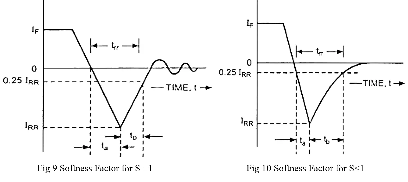
Fig 9 Softness Factor for S =1 Fig 10 Softness Factor for S<1
The peak inverse IRM is expressed as
IRM = ta (di/dt) (1)
Where di/dt is the rate of change of reverse current. The reverse recovery portion looks like a triangle shape. Therefore in order to find the area of the shaded portion. The area of the triangle is applied
QR = 1/2 IRM trr (2)
IRM = (2QR) / trr (3)
If trr ≅ ta
IRM = trr (di/dt) (4)
Equate (3) and (4) equations
(2QR) / trr = trr (di/dt) (5)
trr = [(2QR) / (di/dt)]1/2
if ta =trr then equation (1) become
IRM = trr (di/dt) = [(2QR) / (di/dt)]1/2 . (di/dt) = [(2QR) (di/dt)]1/2
Storage charge and the rate of change of current di/dt affect the peak inverse current and reverse recovery time. The forward diode current IF affects the storage charge.
The key information is often included in the datasheets for power diodes and includes the IF average, IF RMS, VRRM, I2T rating, junction temperature TJ, trr, S-factor, and IRR. In addition to this, there are a lot more graphs and parameters available.
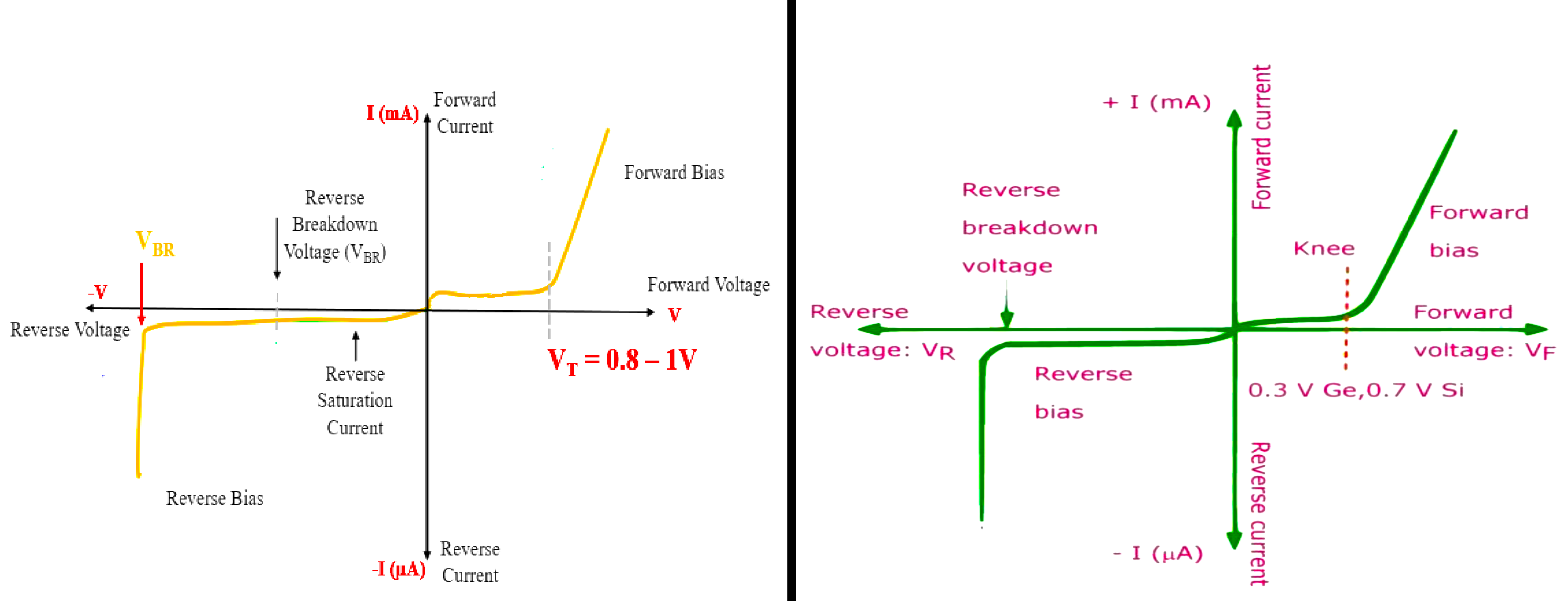
Fig 11 VI Characteristics Comparison Chart between signal and power diode, Image Courtesy: quick-learn
Comparison Between Power Diode and Signal Diode
| S. No | CONVENTIONAL DIODE (SIGNAL DIODE) | POWER DIODE |
| 1 | Voltage, Current, and Power ratings are smaller | P and N are equally doped and it constitutes of only two layers and one junction. |
| 2 | No Drift region is present so doesn’t block higher reverse voltage. | A drift region is part of a power diode. Power diodes are capable of blocking greater reverse voltages due to the drift region’s presence. |
| 3 | The switching speed is lower | Voltage, Current, and Power ratings are larger |
| 4 | It consists of three layers and two junctions with heavily doped P+ and N+. A lightly doped n– layer which is epitaxially grown on a heavily doped layer. | Higher switching speed. |
| 5 | Since Power diodes handle larger current and voltage the size of the power diode is larger. | Compared to signal diodes, power diodes have a larger forward voltage loss. As a result, they take more energy to turn on and use more energy when conducting. |
| 6 | Signal diodes are employed in low-power processes including switching, signal identification, and clipping. | Voltage, Current, and Power rating are smaller |
| 7 | Signal diodes are less in size | Power diodes are employed in rectifiers, power supplies, and other high-current devices. |
| 8 | Signal Diodes lesser cost | Power Diodes are costlier |
Applications of Power Diode
Applications such as high power include three-phase rectifiers, inverters, power controllers, battery chargers, control panel power supply, etc.
Advantages of Power Diode
- When biased in reverse, it may block a large current.
- It offers significantly higher efficiency than typical diodes.
- Power Diode’s ability to sustain a big current for an extended period of time.
Disadvantages of Power Diode
- Power diodes produce more heat than regular diodes, they must always be used with a heat sink.
- Compared to regular diodes, power diodes lose more power.
- Ordinary diodes are less expensive than power diodes.
Reference
- “Power Electronics: Circuits, Devices and Applications” by M H Rashid, Pearson Education
- “ Power Electronics” by P. S. Bimbhra, Khanna Publishers,2012
If you liked this article, then please subscribe to our YouTube Channel for Instrumentation, Electrical, PLC, and SCADA video tutorials.
You can also follow us on Facebook and Twitter to receive daily updates.
Read Next:
- What is Power Electronics?
- SCR Switching Characteristics
- Types of Power Electronic Devices
- Thyristor Interview Questions & Answers
- Power Transistor Structure & Biasing