A transistor is a three-terminal semiconductor device. These devices act as switching devices and are operated at the saturation area, producing a low on-state voltage drop. When a current signal flows to the base or control terminal, they switch on. As long as the control signal is there, the transistor stays on.
Power Transistor
The functioning of a power transistor is identical to that of a regular transistor. The transistor is constructed to handle high voltage and current due to the advantages of traditional power transistors.
The switching speed of transistors is substantially higher than that of thyristors. Low- to medium-power applications employ transistors. Since transistors are current-controlled devices, a constant base current is necessary to maintain their conducting condition.
Types of Transistors
A power transistor is a three-terminal device that is specially made to regulate high current-voltage ratings and handle a wide range of power levels in a device or circuit.
They are divided into two groups based on their structural characteristics: BJT- bipolar junction transistors (transistors like junction transistors, NPN transistors, and PNP transistors) and FET- field-effect transistors (transistors like junction function transistors and metal oxide transistors, N- channel MOSFET, and P- channel MOSFET).
The other types of associated types of transistors are Static induction transistors (SITs), Insulated-gate bipolar transistors (IGBTs). The functionality of transistors is small-signal transistors, Amplifiers, switching transistors, power transistors, high-frequency transistors, phototransistors, etc.
A three-layer, three-terminal device is a bipolar junction transistor. The transistor has three terminals emitter, base, and collector are the three terminals. Collector-base junction (CB) and emitter-base junction (EB) are its two junctions. NPN and PNP transistors are the two kinds of transistors.
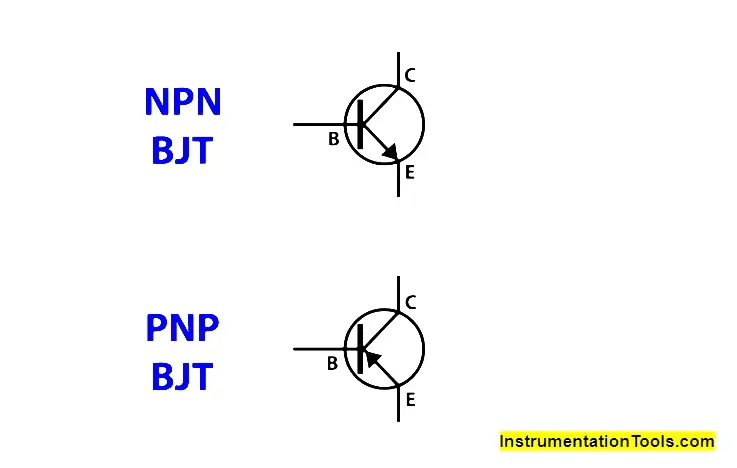
Fig 1 Symbol of Transistor
Power Transistor Structure
The conventional transistor is three terminals, three-layer device. But Power transistor is Four-layer three terminal device. The two-transistor is different in structures. A power transistor is a four-layer device with alternating p- and n-type layers that is vertically orientated. Because it maximizes the cross-sectional area through which the device’s current flows, the vertical construction is recommended.
Additionally, this reduces the on-state resistance and hence the transistor’s power dissipation. Emitter layer and collector layer doping generally amounts to 1019 cm-3. It has a light doping level of 1014 in a specific layer known as the collector drift zone (n–).
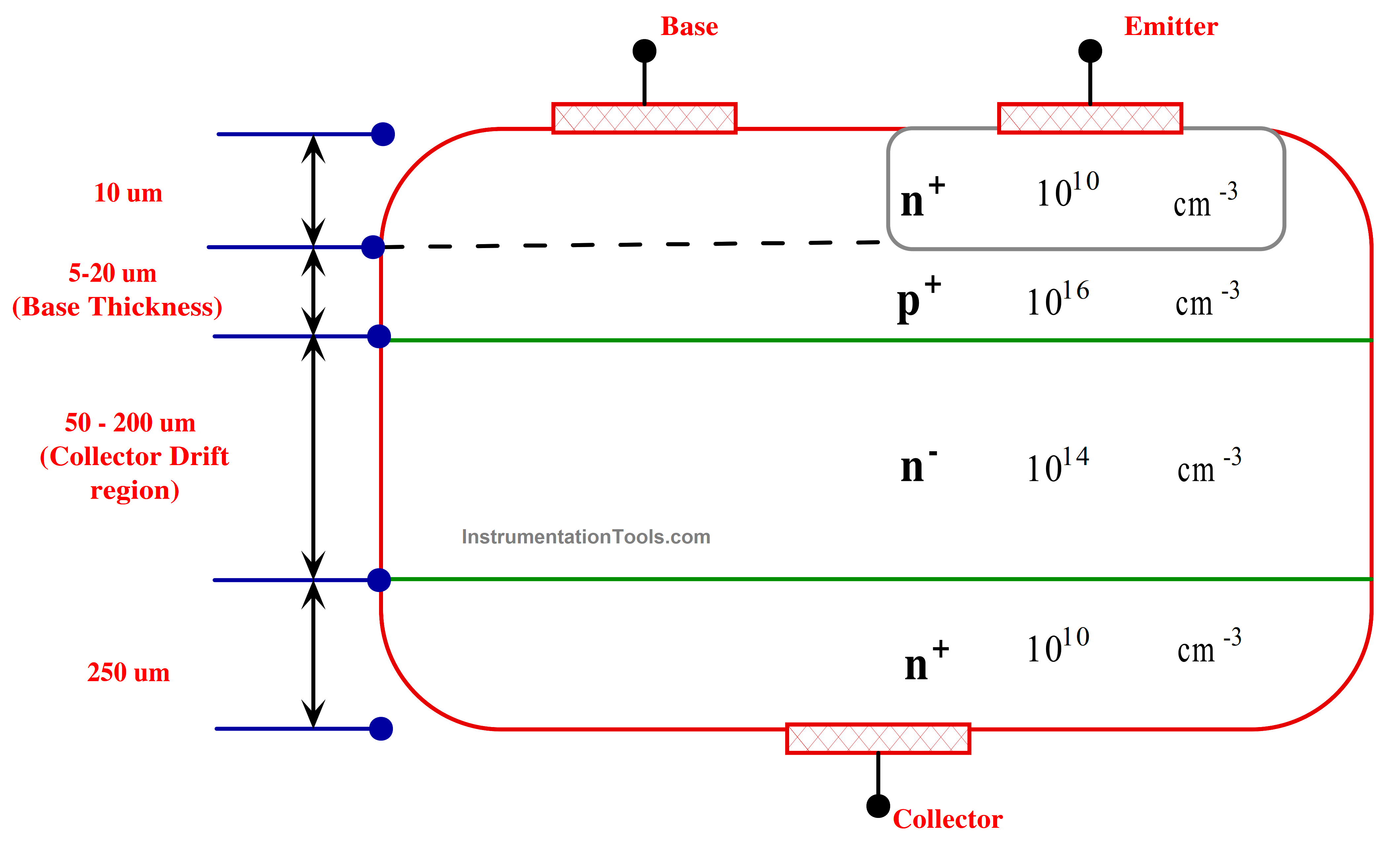
Fig 2 Layer Diagram of NPN Power Transistor
The transistor’s breakdown voltage is dependent on the thickness of the drift area. To have strong amplification capabilities, the base thickness must be as thin as possible, although doing so compromises the transistor’s capacity to withstand a breakdown voltage. Many emitter’s arrangement it lowers the base current path’s parasitic ohmic resistance, which lowers the transistor’s power dissipation.
Biasing
All types of semiconductor devices depend heavily on biassing. This determines the device’s functionality. Most power electronics components function as switches. The same applies to the power transistors also. Using two DC sources, VBB and VCC, biassing in transistor circuits is accomplished.
The most popular techniques for biasing of transistors are the Base Resistor approach, Collector to Base bias, Collector feedback resistor bias, and Voltage-Divider bias.
The fundamental idea behind each of these approaches is to use VCC to derive the needed values of IB and IC in situations of zero signal.
For power transistor works in Common Emitter Configuration. This type of biasing is recommended for higher voltage and current ratings. Since the power transistor is act as a switch in high-voltage and current applications.
Power BJT as Switch
To turn on or off current to a load in logic circuits, a BJT can be utilized as a switching component. The transistor typically operates as a switch in either cutoff (load is OFF) or saturation (load is ON).
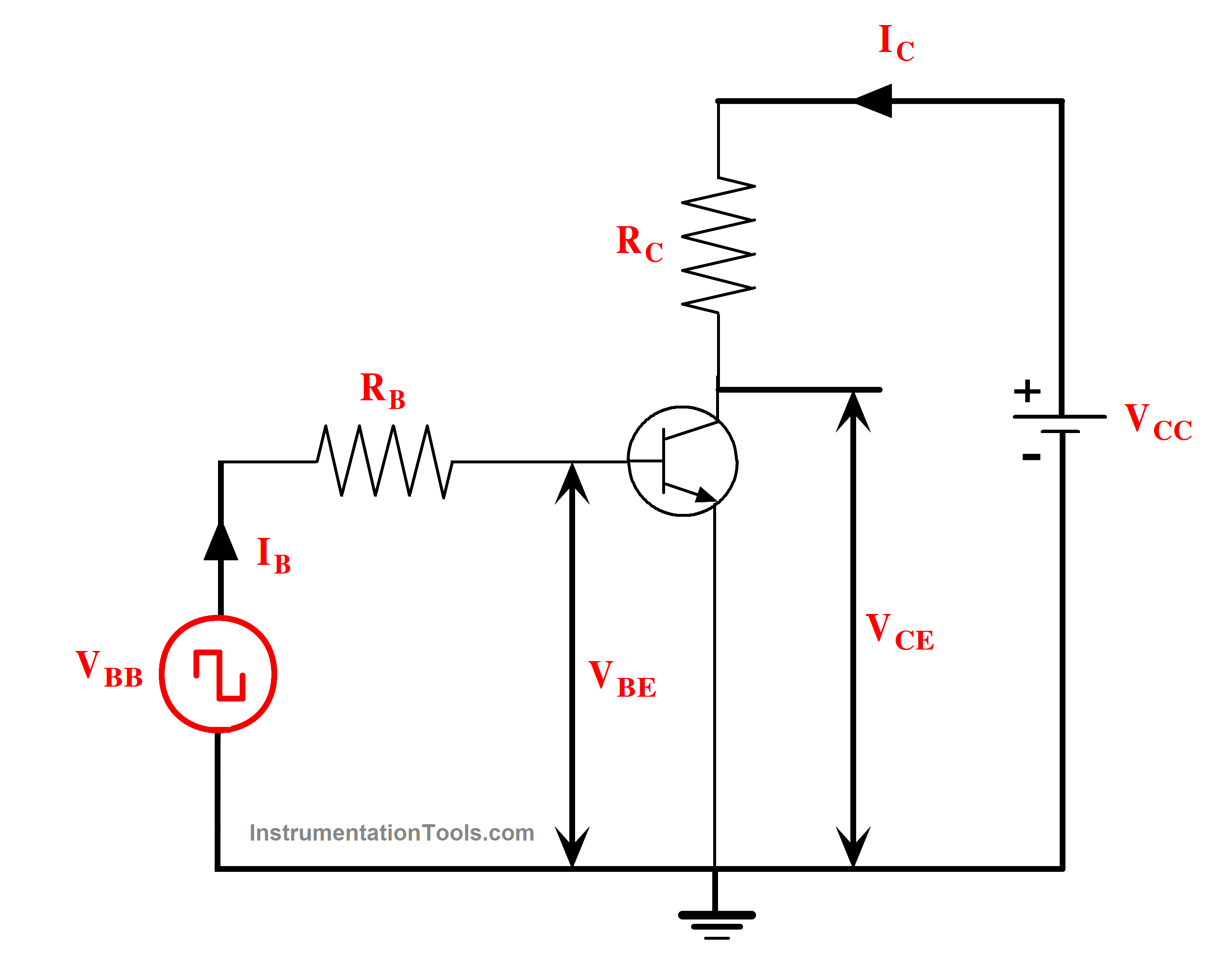
Fig 3 Biasing Circuit of Power Transistor
Input side Equation
Apply KVL
VBB = IB.RB+VBE
IB = (VBB – VBE)/RB
Output side Equation
Apply KVL
VCC = IC.RC+VCE
VCE = VCC – IC.RC
We know that Iβ = IC/IB
IC = IB/ Iβ
BUT, IB = (VBB – VBE)/RB ,
Therefore, VCE
VCE = (VCC – β) . [ {(VCC – VBE).RC }/RB ]
We know that, VCE = VCB+VBE
(OR)
VCB = VCE-VBE
As long VCE>VBE the collector-base junction is reverse biased and transistor works in active region.
When VCB = 0 and VBE =VCE the collector current is maximum in active region
ICMAX = (VCC – VCE)/RC
If IB > IBMAX , Then , VBE and IC increase and VCE falls below VBE. This continues until the BJT enters the saturation area and the Collector-Base junction becomes forward biased.
ODF is defined as the ratio between IB to IBS
ICM = IB / IBS
The ratio of IC to ICS is called forced β
βforced = ICS / IR
The total power loss in the two function is
PT = VBE. IB + VCE IC
Various Notations Used in Power Transistor
| S. No | Notation | Expansion |
| 1 | VBB | Base Voltage |
| 2 | VBE | Emitter to Base Voltage |
| 3 | VCE | Emitter to Collector Voltage |
| 4 | VCC | Collector Voltage |
| 5 | IB | Base Current |
| 6 | IC | Collector Current |
| 7 | ICMAX | Maximum Collector Current |
| 8 | IBMAX | Maximum Base Current |
| 9 | ICS | Saturated Collector Current |
| 10 | IBS | Saturated Base Current |
| 11 | β | Collector to Base Gain |
| 12 | PT | Total Power Loss |
A high value of ODF cannot considerably lower the CE voltage. Power loss increases as VBE rises as a result of the rising base current. The CE voltage does not decrease in reaction to an increase in base current after the transistor is saturated.
When the power is raised at a high ODF value, the transistor might be harmed by thermal runaway. When a transistor is underdriven from IB to IBS, it may function in the active area, which causes VCE to rise and more power loss.
VI Characteristics
The main application of any transistor is Amplifier and Switch. A typical transistor operated in three regions. Cut-off, Active, and Saturation region.
- In the Active region, there will be different base current. So, the collector current increase proportionally with gain Ic = β.Ib.
- In the Cutoff region, the base current is Zero. Therefore, the device behaves as open(No current Flow). It is considered as open Switch
- In the Saturation region, the Base Current is Maximum. The device behaves as a single conductor(i.e., closed switch)
Input Characteristics
The input characteristics are drawn IE Versus VBE by keeping VCE Constant. It operates like a diode at the base-emitter junction. The input characteristics resemble the character curve of PN Junction Forward bias.
For the different values of VCE, the breakdown curve of the BJT varies proportionately.
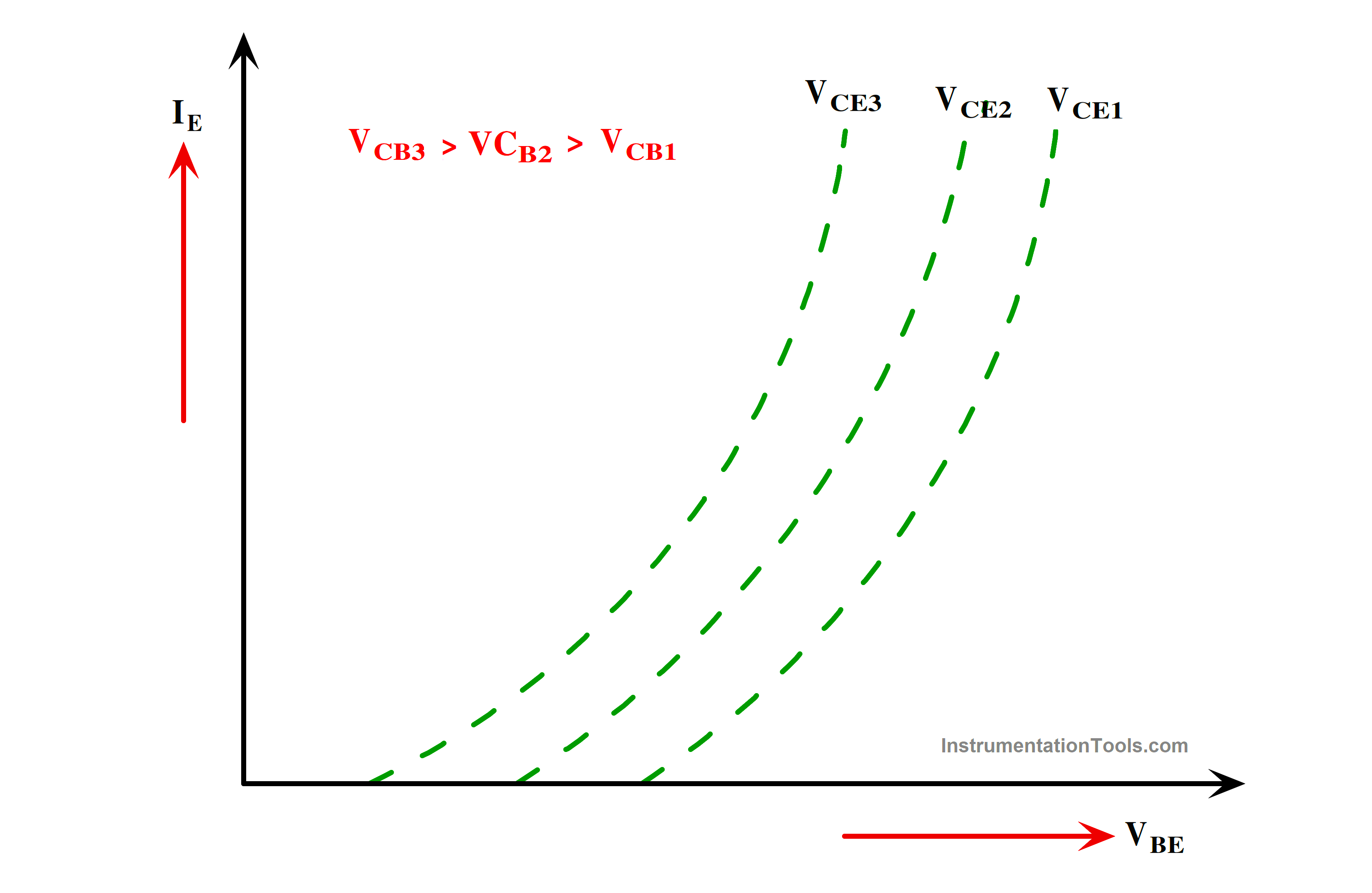
Fig 4 Input Characteristics
Output Characteristics
The output characteristics are drawn VCE versus IC by keeping the different base currents. The base current increased from zero to maximum. The Curve has three regions. Cut-off, Active, and Saturation region.
Cut-Off Region
The collector current (IC) is negligible and the transistor is forced into the cutoff zone when the base current (IB) is zero. In this condition, the transistor is off. The transistor operates as an open switch when it is in the cutoff region, which is also known as the OFF state.
The collector-base and base-emitter junctions are reverse-biased at this time. In this area, the collector-emitter voltage (VCE) is equal to the supply voltage (VCC), and the circuit current is zero.
Active Region
In the active region, different base current is given which is above the threshold i.e base-emitter junction is forward-biased while the collector-base junction is reverse-biased. In this region it the transistor behaves as the amplifier.
Saturation Region
The transistor reaches saturation when the base current is maximum. The transistor behaves like a closed switch when it is saturated because both junctions are forward-biased. Base drive is applied and the transistor is said to be on in quasi- and hard-saturation states. During this condition IC = VCC /RC and VCE = 0.
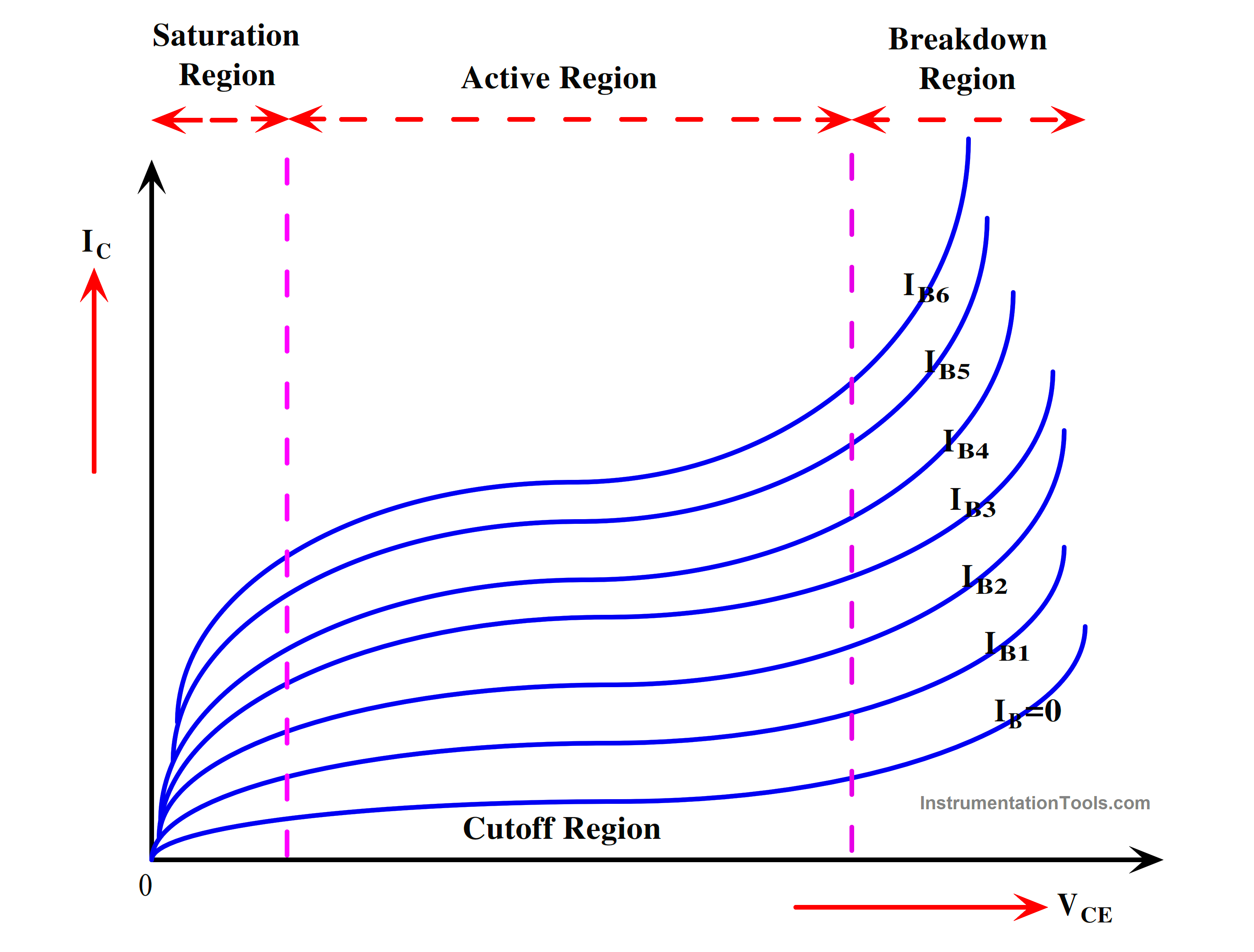
Fig 5 Output Characteristics
Switching Characteristics
A depletion layer capacitance (CCB) and a diffusion capacitance (CBE) may be seen in parallel at a forward-biased p-n junction. Only depletion capacitance exists in a reverse-biased p-n junction.
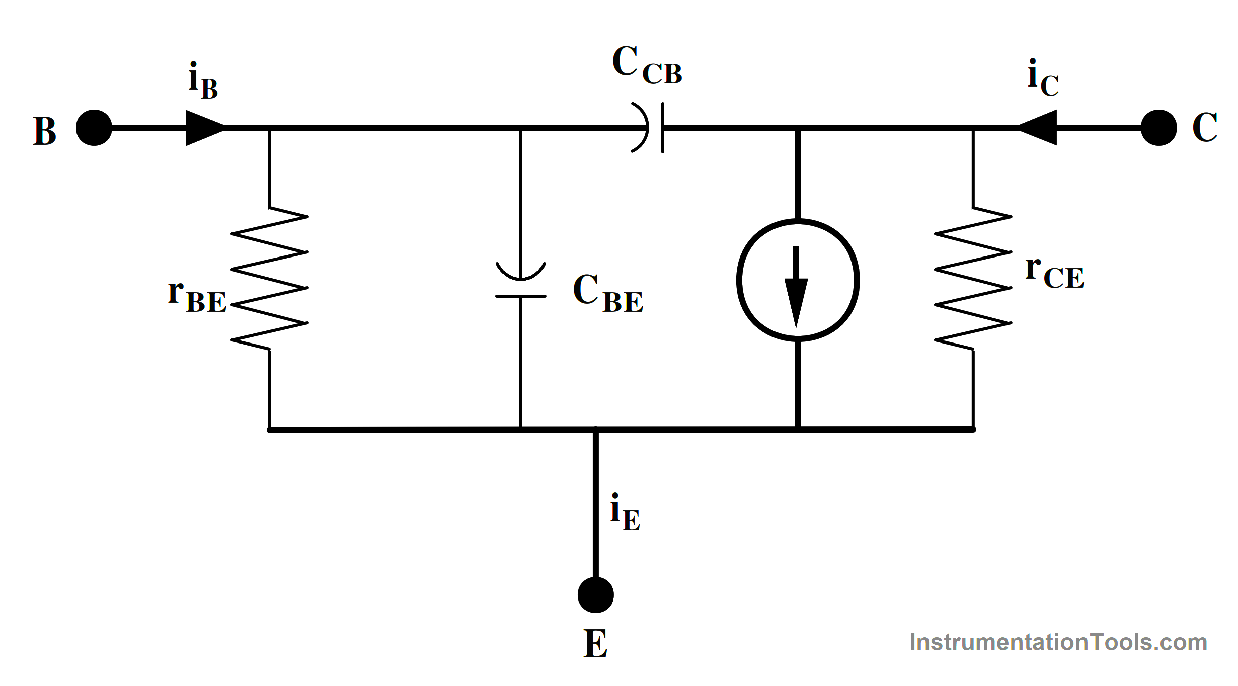
Fig 6 Equivalent Circuit of Power Transistor
The presence of internal capacitance prevents a transistor from turning on instantaneously. Base current increases to IBS when base-emitter voltage VBE is provided, whereas collector current is equal to collector-emitter leakage current ICEO or stays at zero.
The collector current starts to increase after a delay, delay td or delay time. This delay occurs because it takes time to charge the base-emitter capacitance to VBES=0.7 V.
Collector current increases to its steady state value, ICS, in time tr after delay td, which is referred to as the rise time. This indicates that the BJT’s turn-on time is ton=td+tr. The rise time is influenced by the input capacitances.
The collector-emitter voltage tr decreases from VCC to VCES throughout the rising period. In order to sustain forward base current, the transistor remains turned on in a saturated condition.
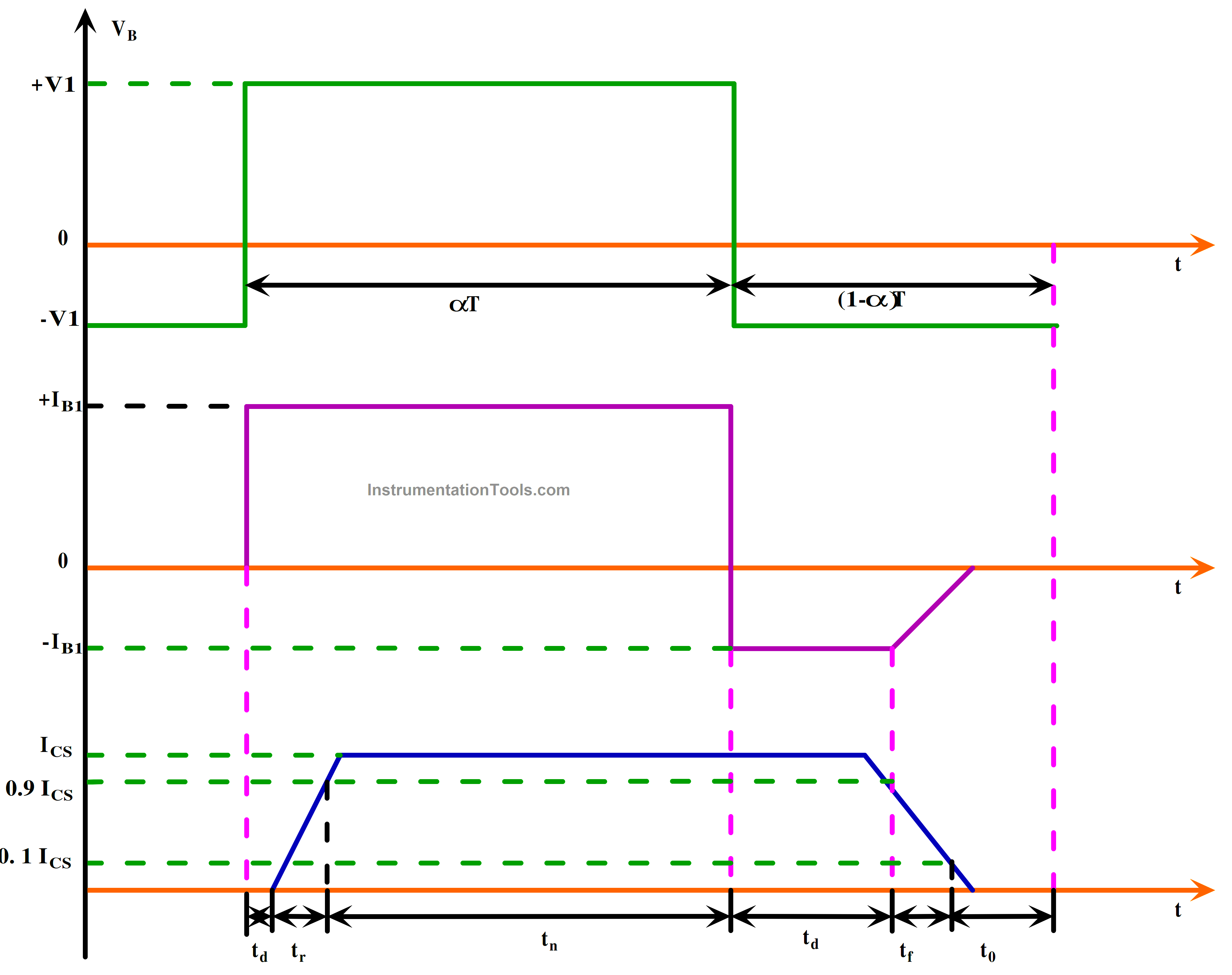
Fig 7 Switching Characteristics of Power Transistor
The collector current does not charge for a period ts, often known as the storage time, after the base-emitter voltage VBE is eliminated at time t1. The base’s saturating charge is eliminated during ts. Collector current starts to decrease time after ts, IC drops to ICEO, and collector-emitter voltage increases to VCC.
The transistor turn-off time, toff=ts+tf, is the sum of the storage time and fall time. The time to is the entire OFF duration, and tn is the steady state duration in the given figure.
Safe Operating Area
The collector current and voltage must always be in this range for the transistor to operate reliably. Actually, the manufacturers FBSOA and RBSOA specify two different forms of SOA.
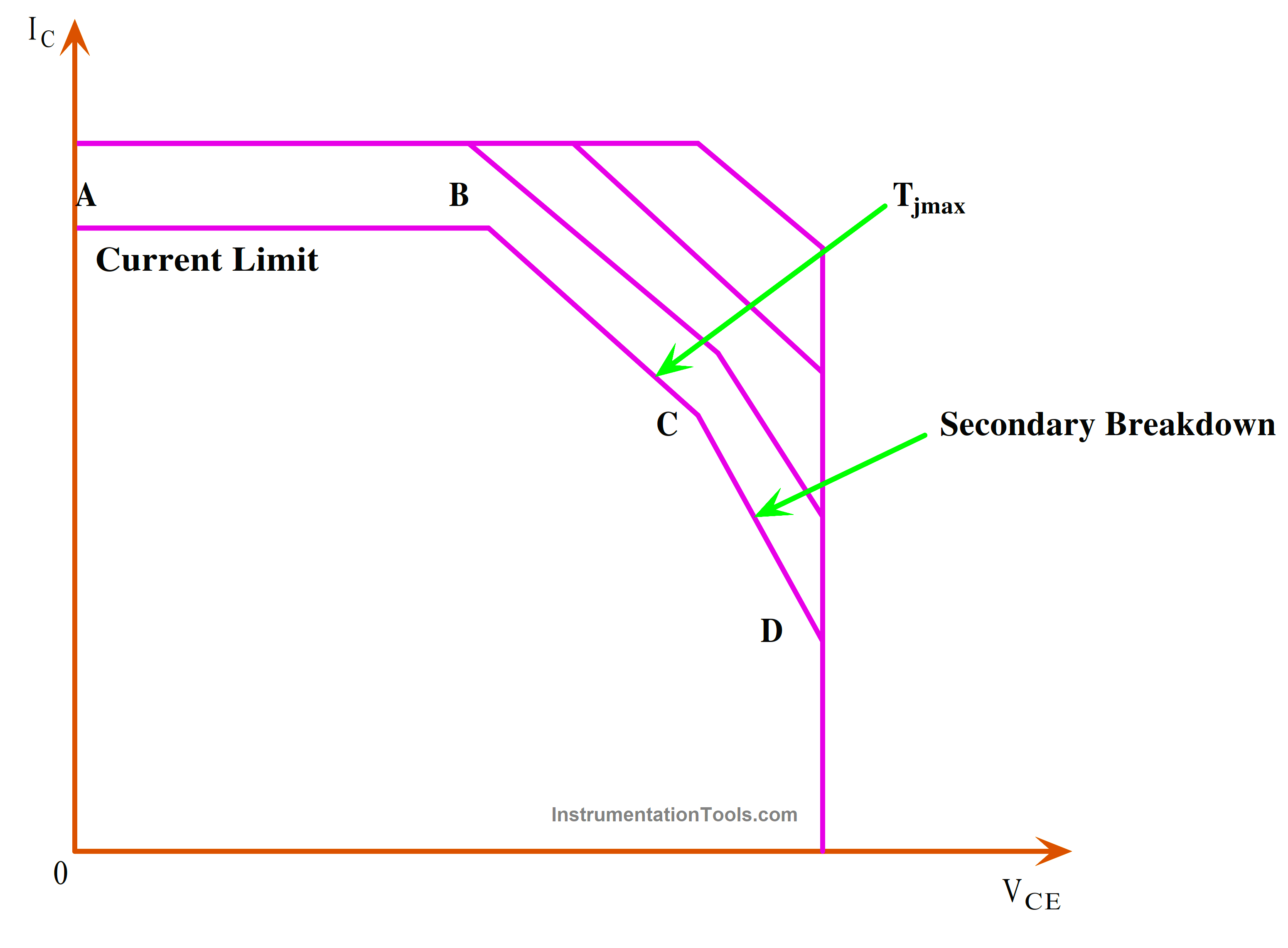
Fig 8 Forward Biased Safe Operating Area (FBSOA)
When the base-emitter junction is forward-biased to turn on the transistor, the transistor operates according to the FBSOA. It is a logarithmic scale.
For VCE less than or equal to 80%, boundary AB is the upper limit for dc and continuous current. Collector current must be lowered to boundary VCE, for VCE greater than 80%. Current should be further decreased in order to prevent secondary breakdown limit and restrict the junction temperature to safe values for further larger VCE.
This secondary breakdown limit is determined by boundary DC. The maximum voltage capacity for this specific transistor is provided by boundary DE. It displays the collector voltage and current combinations that must not be exceeded in order to prevent a second breakdown. This limit also shows as a straight limit on the FBSOA’s log-log scale.
The second breakdown limit differs for “DC” and “Pulsed” operations with various pulse lengths, similar to the maximum power dissipation limit. It is also the same to understand the pulse length as it relates to a certain restriction.
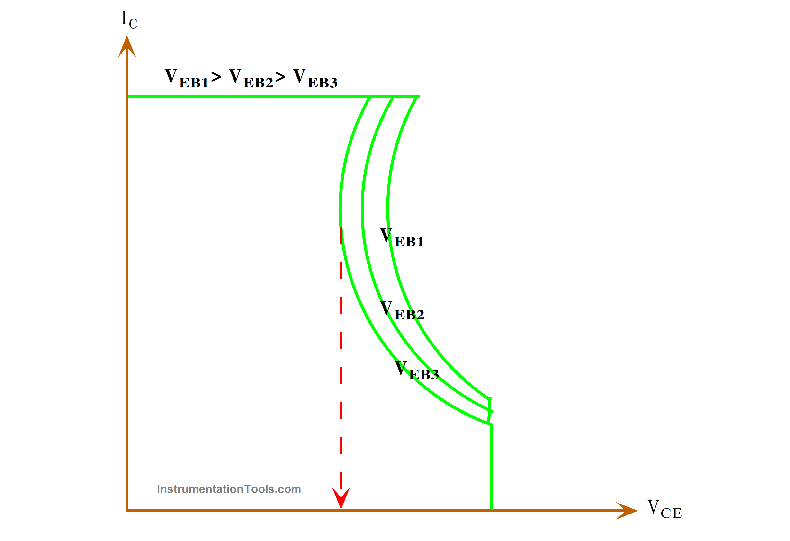
Fig 9 Reverse Biased Safe Operating Area (RBSOA)
A transistor is subjected to increased current and voltage during turn-off, with the base-emitter junction being reverse-biased. Reverse blocking safe operating area, or RBSOA is designated as the safe working region for transistors during shut off. When the base current is zero or the base-emitter junction is reverse-biased during transistor turn-off, this condition is known as RBSO. RBSOA shrinks in size when reverse bias increases.
The RBSOA is more rectangular in form and plotted on a linear scale. Since a transistor cannot conduct current for any meaningful amount of time when it is reverse-biased, RBSOA is a switching SOA. It displays the maximum permitted VCE & IC configurations when the base-emitter junction is reverse-biased. The highest horizontal limit is identical to that in the FBSOA and corresponds to the maximum permitted collector current (ICM).
Advantages of Power Transistor
- The switching frequency range for the power transistor is between 10 and 15 kHz.
- The power transistor may block extremely high voltage while it is off and transport massive currents when it is on.
- Low voltage drops across the power transistor in the ON state.
- The power transistor is extremely simple to ON and OFF.
- It may be used to regulate the amount of power sent to the load, inverters, and helicopters.
Disadvantages of Power Transistor
- The power transistor has a very low reverse-blocking capability.
- Above a switching frequency of 15 kHz, the power transistor cannot function effectively.
- It could sustain thermal runway damage or a subsequent collapse.
Applications of Power Transistor
- Switch mode power supply
- Relay drivers
- DC motor speed control
- Lighting systems
- PWM applications
Reference
- “Power Electronics: Circuits, Devices and Applications“, M H Rashid, Pearson Education
- “ Power Electronics” P. S. Bimbhra, Khanna Publishers, 2012
If you liked this article, then please subscribe to our YouTube Channel for Instrumentation, Electrical, PLC, and SCADA video tutorials.
You can also follow us on Facebook and Twitter to receive daily updates.
Read Next:
- What is Power Electronics?
- SCR Switching Characteristics
- Types of Power Electronic Devices
- Power Diode Characteristics
- Thyristor Interview Questions & Answers