The switching characteristics of a thyristor refer to its behavior during the switching process, specifically when it transitions between the off state (non-conducting) to the on state (conducting) and vice versa.
These characteristics are essential to understand for designing and controlling circuits that use thyristors. Here are some key switching characteristics of a thyristor:
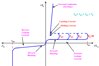
Switching Characteristics of Thyristor
Once the Thyristor is switched ON, the gates losses its control. The device will be turned OFF only bringing the thyristor below the holding current.
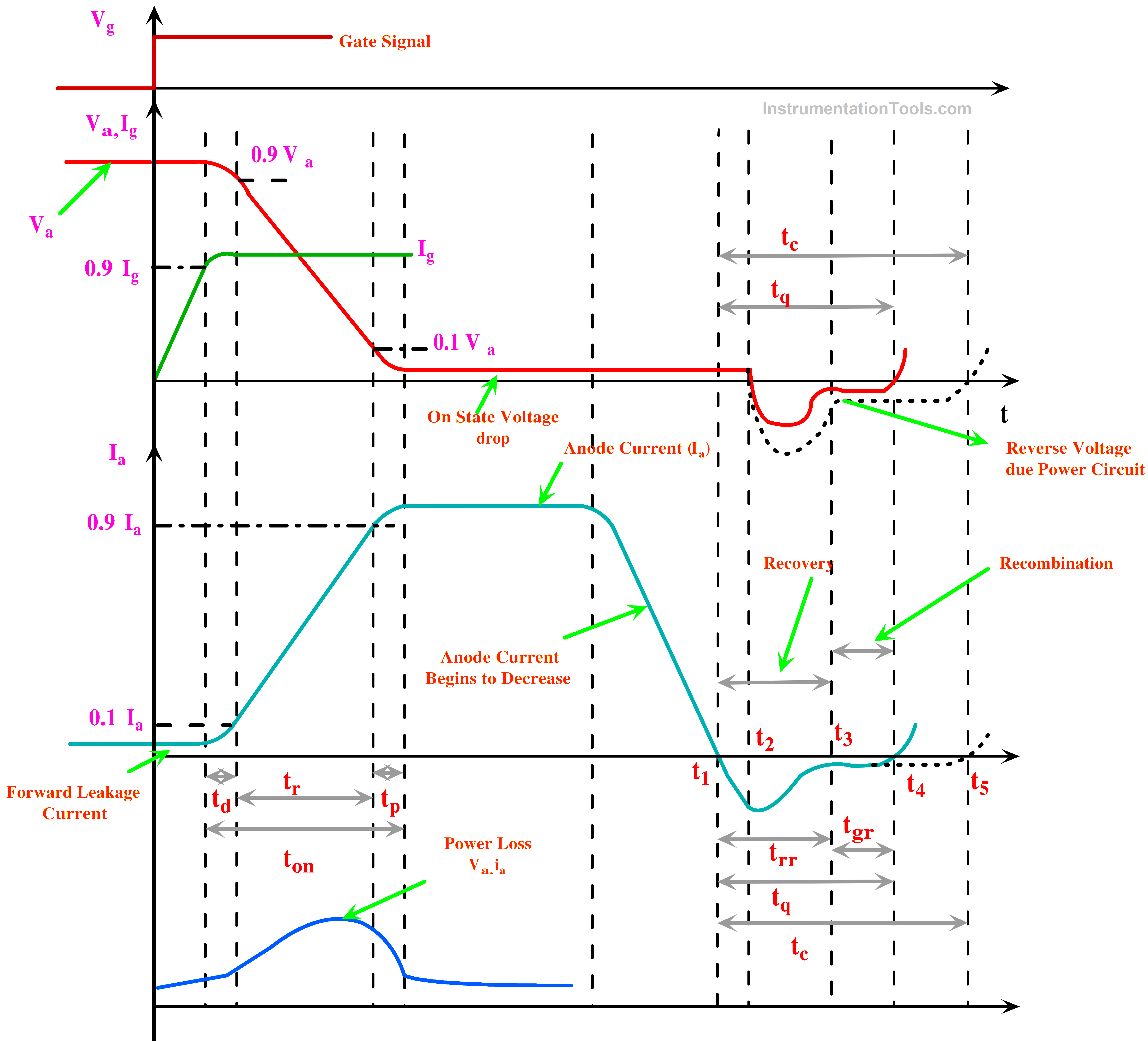
Fig 1 – Switching Characteristics of Thyristor
Turn ON time of the Thyristor
There are three segments that make up total turn-on time: delay, rise, and spread times.
Delay time(td)
The delay time of a thyristor, also known as the turn-on time or firing delay, refers to the time it takes for the thyristor to switch from the off state to the on state once a trigger signal or gate current is applied.
In this the device will be turned once the Gate current of the thyristor reaches above the threshold level i.e. the gate increases from 0.9Ig to Ig, during this time the device is ready to conduct therefore the anode Voltage (Va) starts to decrease for Va to 0.9Va. By applying high gate current the time taken for delay can be reduced further.
Rise Time (tr)
The rise time is the time it takes for the thyristor to transition from a non-conducting state to a fully conducting state. It is influenced by the rate at which the thyristor’s internal junctions turn on and reach their rated voltage.
The rise time can vary significantly depending on the specific thyristor model and its characteristics but is typically in the range of microseconds to milliseconds. Rise time is also referred to as the rate of rise of anode current from 0.1Ia to 0.9Ia.
The gate current’s amplitude and build-up rate have an inverse relationship with the rising time. As a result, tr can be decreased by applying the gate to high and steep current pulses.
Due to high anode voltage (Va) and significant anode Current (Ia) occurring simultaneously in the thyristor during rising time, turn-on losses in the device are at their maximum. Local hot spots may arise and the gadget may become damaged because these losses only affect a tiny conducting region.
Spread Time (tp)
The cross-section of the thyristors will be covered by the electrons during the spread time. The distance between the cathode and gate affects the spreading time. After the spread time, the anode current reaches its steady state; typically, the on-state voltage drop is substantially lower.
The total turn ON time ton is the sum of delay time plus rise time plus spread time.
Ton = td + tr + tp
SCRs could be categorized as charge-controlled devices when they are turned on. For the thyristor conduction to start, a specific quantity of charge must be introduced into the gate region. The gate current’s value has a direct correlation with this charge.
Therefore, the faster this charge is injected, the bigger the gate current’s magnitude. Therefore, employing larger gate current values will shorten the turn-on time. Typically, the gate current is 3 to 5 times more than the gate current needed to trigger an SCR.
A thyristor is considered to be hard-fired or overdriven when the gate current is significantly higher than the minimal gate current necessary. A thyristor’s turn-on time is shortened and its di/dt capability is improved by hard firing or overdriving. This waveform features a faster rising time and a higher beginning value of gate current. In order to prevent an unintentional device turn-off, the gate current is first lowered from its high beginning value to a lower value where it remains for a number of microseconds.
Turn OFF time of the Thyristor
Thyristor turn-off denotes a change from the on to the off state and the ability to avoid forward voltage. The commutation process or turn-off process refers to the dynamic transition of the SCR from the conduction state to the forward blocking state.
The gate loses control once the thyristor is turned on. By lowering the anode current below the holding current, the SCR can be disabled. The SCR won’t be able to block forward voltage if it is provided to it at the same instant that the anode current drops to zero because the carriers (holes and electrons) in the four layers are still conducive to conduction. Therefore, even if there is no gate signal applied, the device will immediately enter conduction. The thyristor must be reverse-biased for a limited time after the anode current reaches zero in order to prevent such an occurrence.
The interval between the moment the anode current drops to zero and the moment the SCR regains its capacity to block forward is known as the turn-off time (tq) of a thyristor. All of the extra carriers from the four layers of the SCR must be eliminated within time tq.
In order to get rid of the extra carriers, holes from the outer p-layer and electrons from the outer n-layer are swept out. Only by recombination can the carriers around junction J2 be eliminated. The turn-off time is composed of two intervals: the gate recovery time (tgr) and the reverse recovery time (trr).
tq=trr + tgr
The anode current reaches zero at moment t1. The existence of carriers stored in the four layers is the cause of the anode current reversal after time t1. During the interval between instants t1 and t3, the reverse recovery currents clear out extra carriers from the end junctions J1 and J3. The sweeping out of holes from the top p-layer and electrons from the bottom n-layer, in other words, causes reverse recovery current to flow.
At instant t2, as approximately 60% of the stored charges are released from the top two layers, the carrier density across layers J1 and J3 starts to decline, and the reverse recovery current also begins to degrade at this time.
When the reverse recovery current reaches almost zero at instant t3, the end junctions J1 and J3 recover, allowing the SCR to block the reverse voltage. The reverse recovery behavior for a thyristor between t1 and t3 resembles that of a rectifier diode.
The middle junction J2 still retains trapped charges at the end of the reverse recovery phase (t3 — t1), therefore the thyristor is unable to block the forward voltage at that time. The trapped charges at J21, namely in the inner two layers, are unable to flow to the external circuit and can only degrade by recombination. If a reverse voltage is kept across the SCR, this recombination is feasible, however, the amount of this voltage is not crucial.
The parameters of the external circuit have no effect on the rate of charge recombination. Gate recovery time (tr) is the period of time between t3 and t4 during which charges recombine. The forward voltage between the anode and the cathode can be applied again at instant t4 when junction J2 recovers.
Since their recombination takes longer, the turn-off time is also longer. This is due to the quicker rate at which high reverse voltage draws the carriers from junctions J1, J3, and the nearby transition areas. An individual SCR is affected by the thyristor turn-off time tq.
In actuality, a thyristor (or thyristors) is a component of the power circuit. Circuit turn-off time (tc) refers to the turn-off time that the practical circuit supplies to the thyristor. For a device to reliably turn off, time tc must be longer than time tq; otherwise, commutation failure, when the device turns on unexpectedly, may occur.
The turn-off period of thyristor is comparatively higher than any other device. This is due to the trapped charges. The thyristor once conducted, the gate loses its control. Due to this reason, the device turn-off time is complicated.
Two Transistor Model of Thyristor
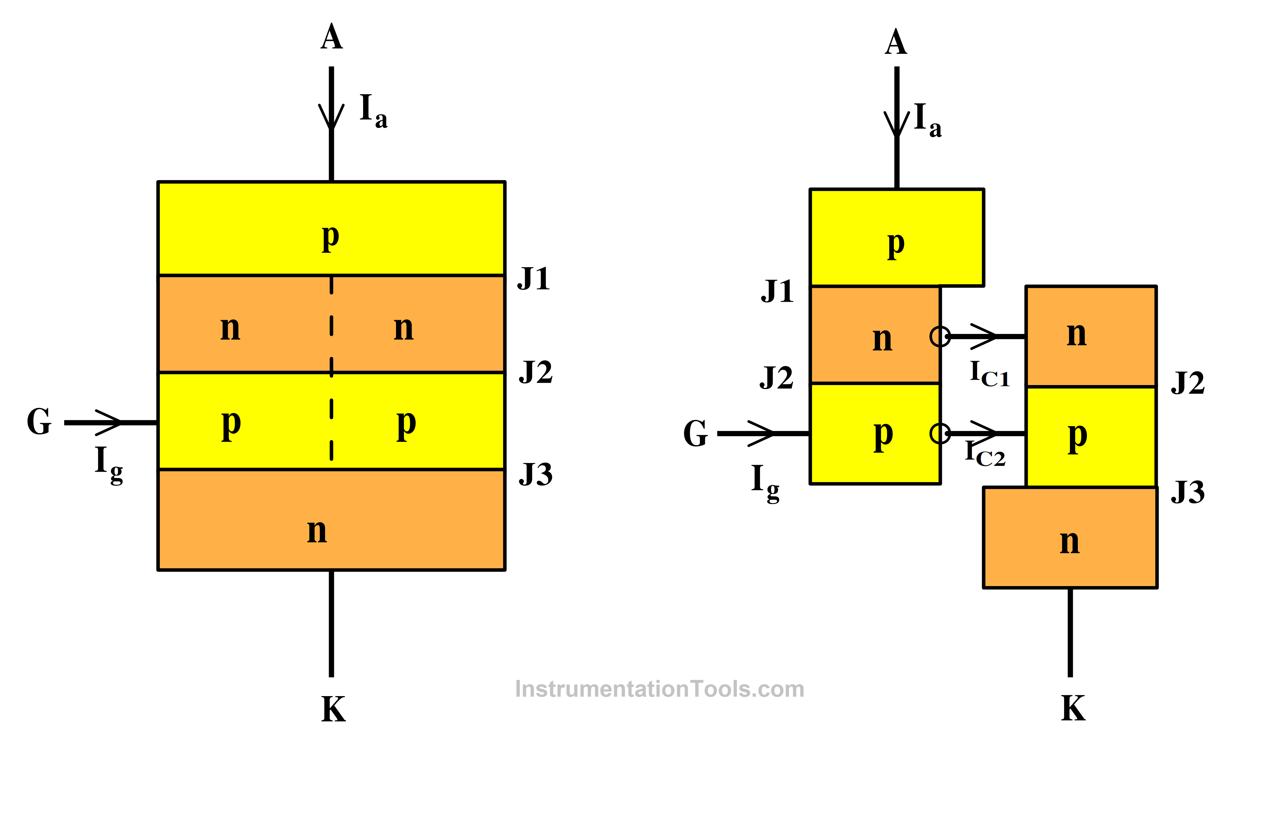
Fig A (Left) – Thyristor Layer Diagram Fig B (Right) – Two Transistor Model
The two-transistor model of thyristor activity can be explained by its fundamental workings. Fig depicts the schematic of a two-transistor thyristor model.
This is achieved by cutting the two middle layers in half along the dotted line, as shown in Fig. You can think about the junctions J1—J2 and J2–J3 as making up distinct pnp and npn transistors.
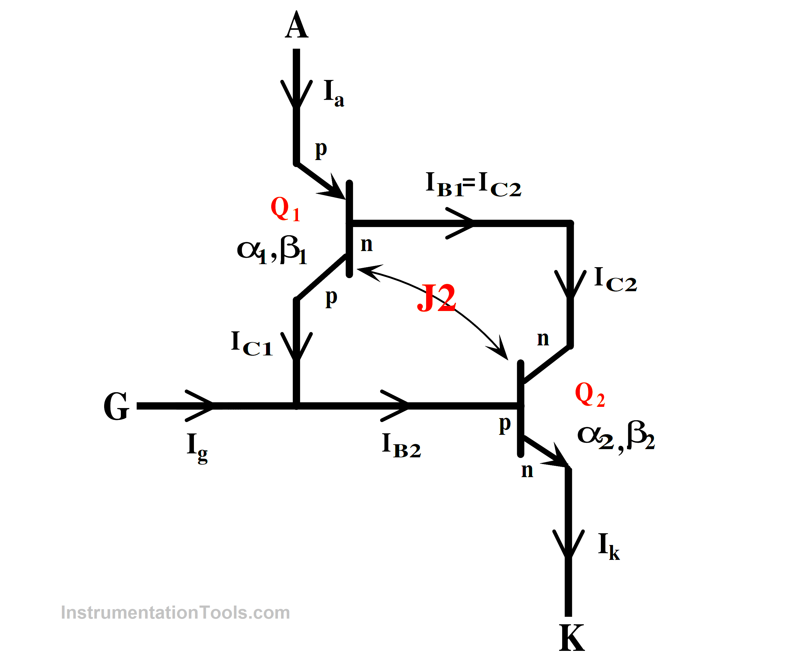
Fig C. Schematic of Two Transistor Model.
A transistor’s collector current (IC) and emitter current (IE) are connected in the off state as follows:
IC = αIE +ICBO
Where “α” is a transistor’s common base current gain and ICBO is its common base leakage current at the collector base Junction
In the case of transistor Q1, the anode current Ia and the collector current Ic are the same. As a result, for Q1
IC1 = α1Ia +ICBO1 (1)
where
α1 = Q1 common base current gain.
ICBO1 = Q1 common base leakage current.
Similarly, the collector current IC2 for transistor Q2 is given by
IC2 = α2Ik +ICBO2 (2)
Where,
α2 = Q2 common base current gain.
ICBO2 = Q2 common base leakage current.
Ik = Q2 emitter current.
The external circuit current Ia entering at anode terminal A is equal to the total of the two collector currents provided by Equ. (1) and (2).
Ia= ICl + IC2 (3)
Ia = α1Ia +ICBO1+ α2Ik +ICBO2
Ik = Ia + Ig when gate current is applied. When this value of Ik is substituted in Equ. (3),
Ia = α1Ia +ICBO1+ α2 (Ia+Ig) +ICBO2
Ia = (α1Ig +ICBO1+ICBO2) / ( 1 – {α1 + α2}) (4)
Current gain α for a silicon transistor is extremely low at low emitter current. Rapid buildup occurs with an increase in emitter current. When the thyristor is forward biased and the gate current is set to zero, the forward leakage current flows somewhat more than (ICBO1+ICBO2).
If there is a way to increase the emitter current of two component transistors such that (α1+α2) approaches unity, then Equ 4. Ia would have a tendency to reach infinity, by turning on the device.
Actually, after the thyristor starts conducting, an external load restricts the anode current to a safe level. In reality, the techniques for activating a thyristor are the techniques for getting (α1+α2) to approach unity.
Advantages of Thyristors
- Thyristor switches have a number of advantages over mechanical switches, including the ability to operate at high frequencies, reduced space requirements, ease of use for complex control, high power handling capacity, and use as a controlled rectifier in AC circuits.
- They can also handle high voltages and currents and act as protection devices similar to fuses in power lines.
Disadvantages of Thyristors
- The thyristor must be activated every cycle in an AC circuit.
- The on- and off-time of SCR is lengthy.
- The load may be delayed or damaged as a result.
- When attached, it can halt the motor, but it cannot keep it still.
- Thyristor has a relatively low response rate.
- DC circuits are not very useful because the thyristor cannot be turned off by simply disconnecting the gate drive.
- In GTO Thyristor, latching and holding current is more important. The voltage’s ability to block reverse current is less than its ability to stop forward current.
Applications of Thyristors
Thyristors are frequently employed in a wide range of applications, such as:
- Controlling the voltage and current of AC circuits, such as those in dimmer switches, motors, and heating elements, is known as power control.
- Power electronics inverters and converters are used to convert DC to AC or AC to DC.
- Surge protectors and overvoltage protection circuits are examples of protective devices.
- Switching High-Power Loads: In situations when switching at high voltages and currents is necessary.
Reference
- “ Power Electronics” P. S. Bimbhra, Khanna Publishers, 2012
- “Power Electronics: Circuits, Devices and Applications“, M H Rashid, Pearson Education
If you liked this article, then please subscribe to our YouTube Channel for Instrumentation, Electrical, PLC, and SCADA video tutorials.
You can also follow us on Facebook and Twitter to receive daily updates.
Read Next:
- Power MOSFET – Symbol, Types
- How to test SCR using a Multimeter
- MCT (MOS Controlled Thyristor)
- SCR Triggering Methods Explained
- Types of Power Electronic Devices