IGBT (Insulated Gate Bipolar Transistor) is a type of semiconductor device that combines the characteristics of both bipolar junction transistors (BJTs) and metal-oxide-semiconductor field-effect transistors (MOSFETs).
IGBT (Insulated Gate Bipolar Transistor)
IGBT is widely used in various electronic applications, especially in power electronics and high-voltage systems. IGBTs are designed to handle high voltages and currents while providing the switching speed of a MOSFET and the current-carrying capability of a BJT. IGBTs with symmetrical and asymmetrical structures are another name for these devices.
Similar to MOSFETs, an IGBT has a high input impedance, whereas a BJT has a low on-state conduction loss. However, unlike with BJT, there is no second breakdown issue. The corresponding drain-to-source resistance RDS is regulated by chip design and structure to behave like that of a BJT.
IGBT Symbol
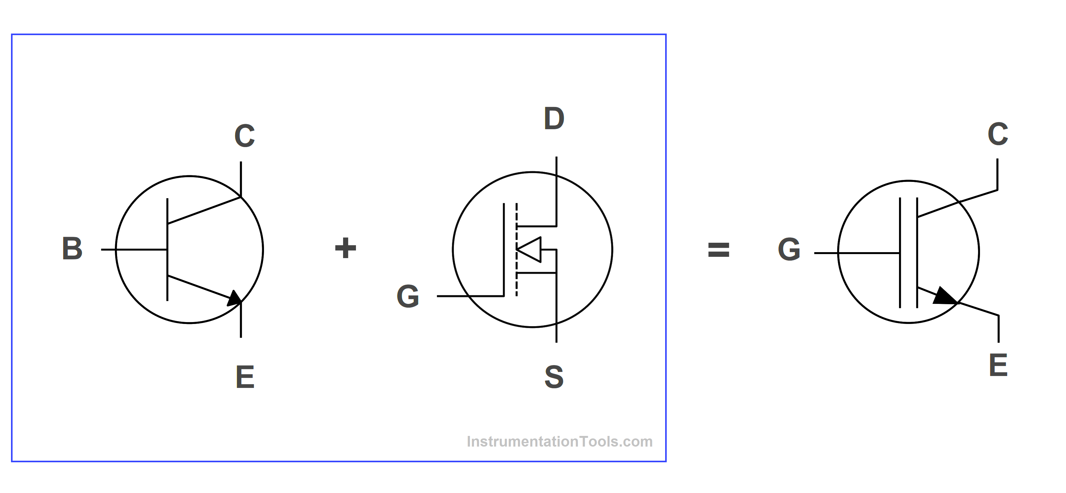
Fig 1. Symbol and Equivalent of IGBT
Types of IGBT
Typically, two varieties of Insulated Gate Bipolar Junction Transistors (IGBT) exist.
- Non-Punch Through IGBT [NPT-IGBT]
- Punch Through [PT-IGBT].
The PT IGBT construction uses a strongly doped n-buffer layer in the drift region close to the collector to shorten switching times. The drift region’s conductivity is modulated in the NPT structure, which lowers the on-state voltage drop and maintains carrier lifetime above that of a PT structure. Similar to a power MOSFET, an IGBT is a voltage-controlled electronic component. as in a MOSFET.
An IGBT with identical forward and reverse breakdown voltages is referred to as an NPT-IGBT Symmetrical IGBT. These devices are employed in AC applications.
The reverse breakdown voltage of asymmetrical IGBTs (PT-IGBT) is lower than the forward breakdown voltage. These IGBTs are beneficial for DC circuits since they don’t need to sustain voltage flowing in the opposite direction.
The n carriers are attracted into the p-channel close to the gate area when the gate is made positive with respect to the emitter for turn-on. This results in a forward bias of the base of the NPN transistor, which turns on. voltage to close the channel. such as durability, capability, peak current, and simplicity of gate drive.
Inherently, an IGBT is quicker than a BJT. IGBT switching speeds, however, are slower than MOSFET switching speeds. Fig depicts the IGBT’s biassing circuit. As opposed to the gate, drain, and source for a MOSFET, the three terminals are the gate, collector, and emitter. Fig depicts the usual production and transfer characteristics.
Construction Details of IGBT
A p+ layer substrate serves as a base for an IGBT. An epitaxially formed high resistivity n- layer is generated on a p+ substrate. The IGBT’s capacity to block voltage is determined by the thickness of the n-layer, which is known as the drift region, much like in other semiconductor devices.
The Collector (C) terminal is created by depositing a metal layer on the opposite side of the p+ substrate. The epitaxially formed n- layer now has dispersed p regions. In the p area, n+ regions are also spread.
The Fig shown below depicts the fundamental architecture of an IGBT. Silicon Dioxide (SiO2) is now being developed on the surface as an insulating layer. Metal Emitter and Gate terminals are carved into this insulating layer. Since the p+ substrate injects holes into the n– layer, it is also known as the injector layer.
The drift zone refers to the n– layer. The body of the IGBT is the next p layer. The p n– junction’s J2 depletion layer is accommodated by the n– layer that lies between the p+ and p regions.
Working of IGBT
At first, assume that there is no voltage provided to the Gate terminal; the IGBT will be in a non-conductive condition at this point.
The negative ions will now collect on the top side of the SiO2 layer and the positive ions will accumulate on the bottom side of the layer when the applied gate voltage is increased owing to the capacitance effect on the SiO2 layer.
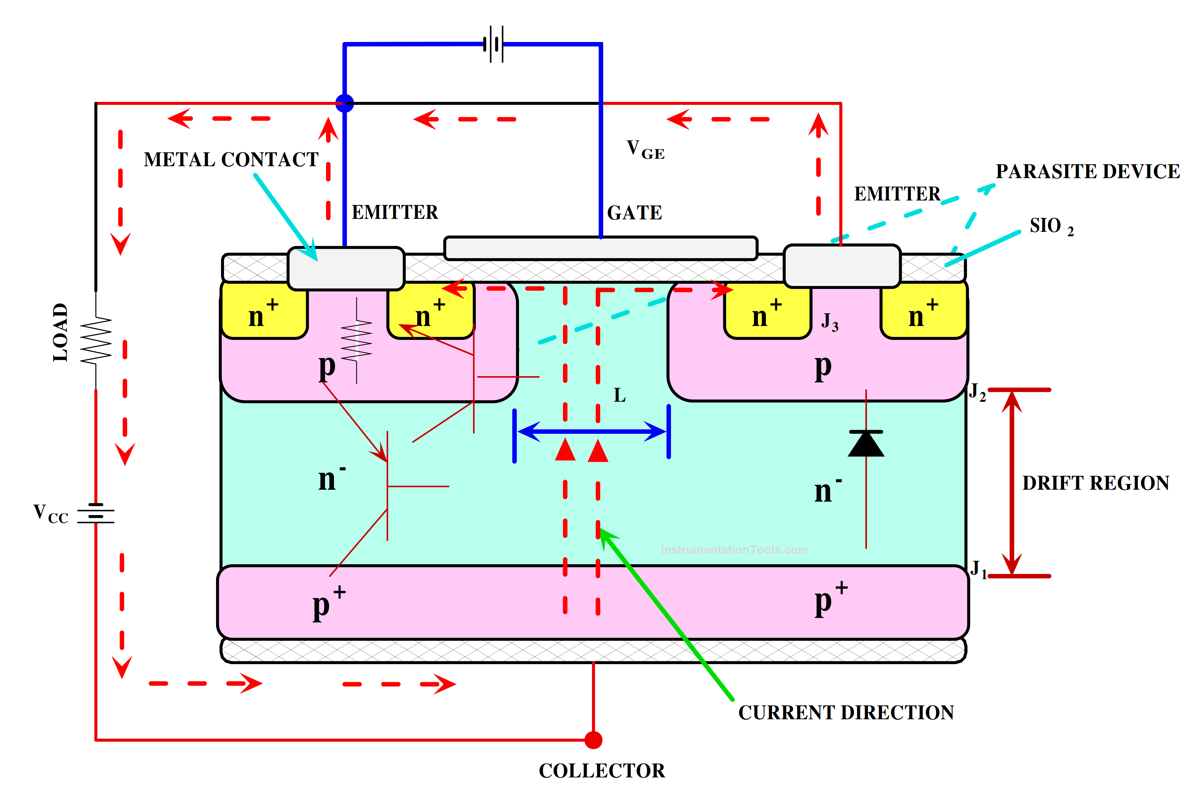
Fig 2 Layer Diagram of IGBT
As in a power MOSFET, an n channel forms in the p regions when the gate is positive with respect to the emitter and with a gate-emitter voltage greater than the threshold voltage of the IGBT. The n channel short connects the n– region with n+ emitter regions.
Substation holes are injected into the epitaxial n– layer from the p+ substrate layer as a result of an electron movement in the n channel. Eventually, a forward current forms, as seen in Fig.
A PNP transistor is made up of three layers: p+ acts as the emitter, n– as the base, and p as the collector. NPN transistors are also made up of n–, p, and n+ layers, as seen in Fig Here, n– functions as both the PNP transistor’s base and the NPN transistor’s collector.
Additionally, p functions as the base of the NPN transistor as well as the collector for PNP devices. Therefore, it is possible to link the two PNP and NPN transistors.
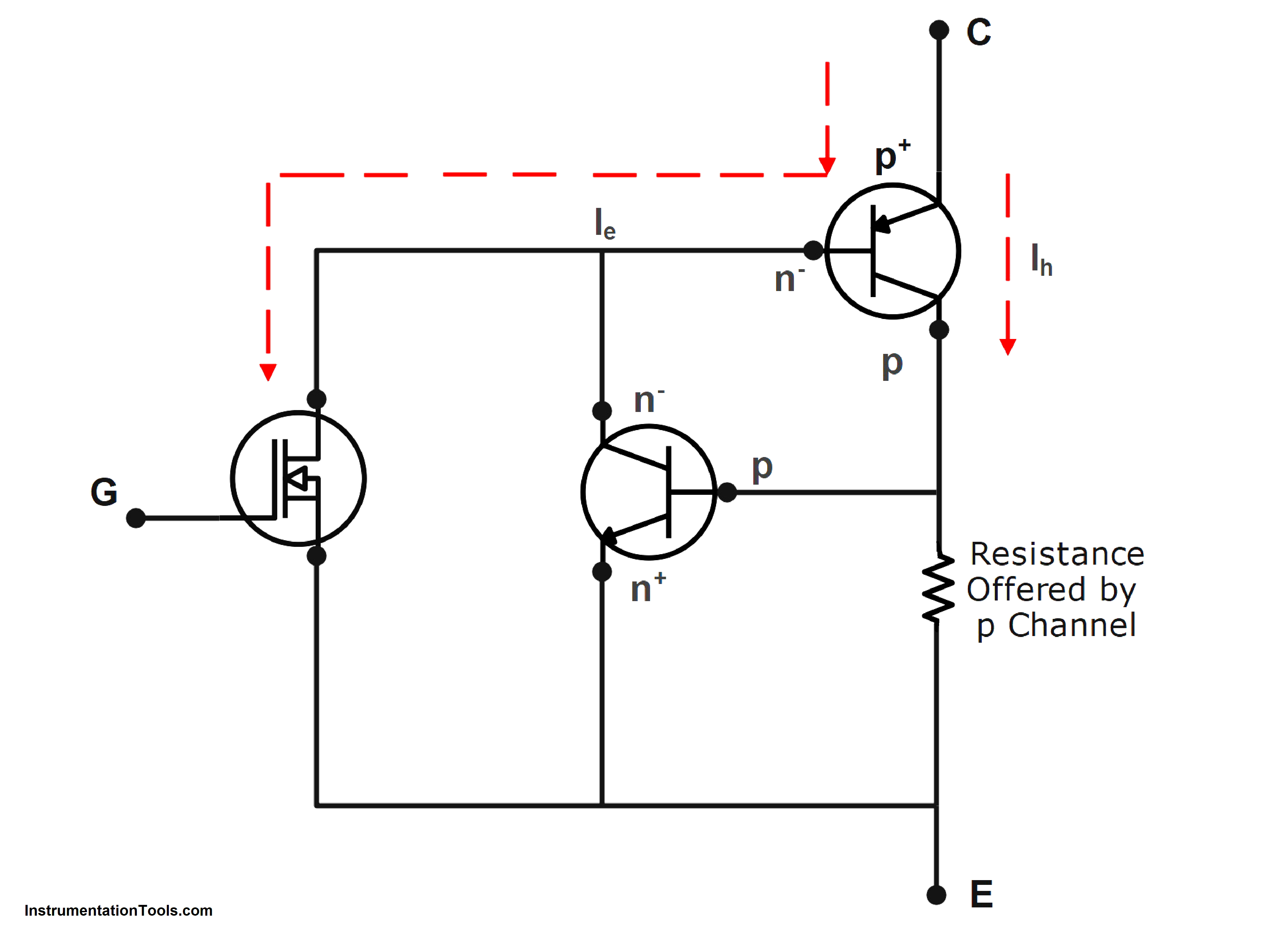
Fig 3 Equivalent Circuit of IGBT
The Collector current of IGBT resolved into two components Ie and Ih.
- Hole current Ih is brought on by the injection of holes from the emitter, p+ n– p transistor Q1, p+ n collector, and p-body region resistance Rp.
- Electronic current Ie is caused by injected electrons that are flowing from the emitter, injection layer p+, drift zone n–, and collector.
Ic= Ih + Ie
An IGBT undergoes three voltage drops when it is turned on: one in the n-channel, one across the drift n-region, and one across the forward-biased p+n junction J1.
In the range of 0.7 to 1V, the voltage drop across junction J1 is extremely tiny. IGBTs have very low ON-state voltage drops, which results in reduced ON-state losses.
VI Characteristics of IGBT
The IGBT VI characteristics are similar to the characteristics of MOSFET. The biasing circuit and VI characteristics are shown below.
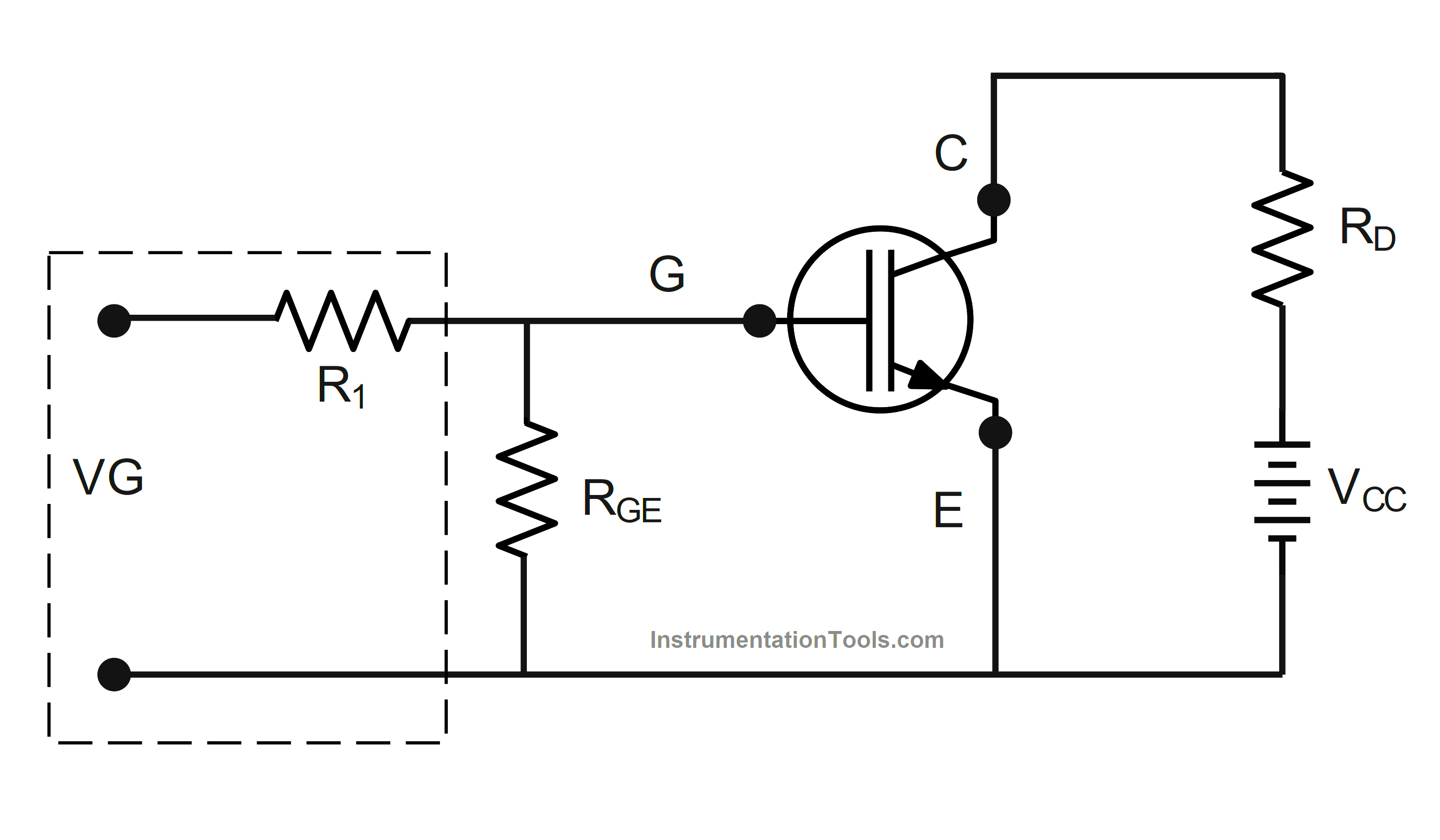
Fig 4. Biasing Circuit of IGBT
The VI Characteristics divided into Transfer or Input characteristics and Output Characteristics
Transfer Characteristics
The plot of collector current (IC) vs. gate-emitter voltage (VGE) represents an IGBT’s transfer characteristics. This characteristic is the same as that of a power MOSFET. VGET is in the off state when VGE is less than the threshold voltage.
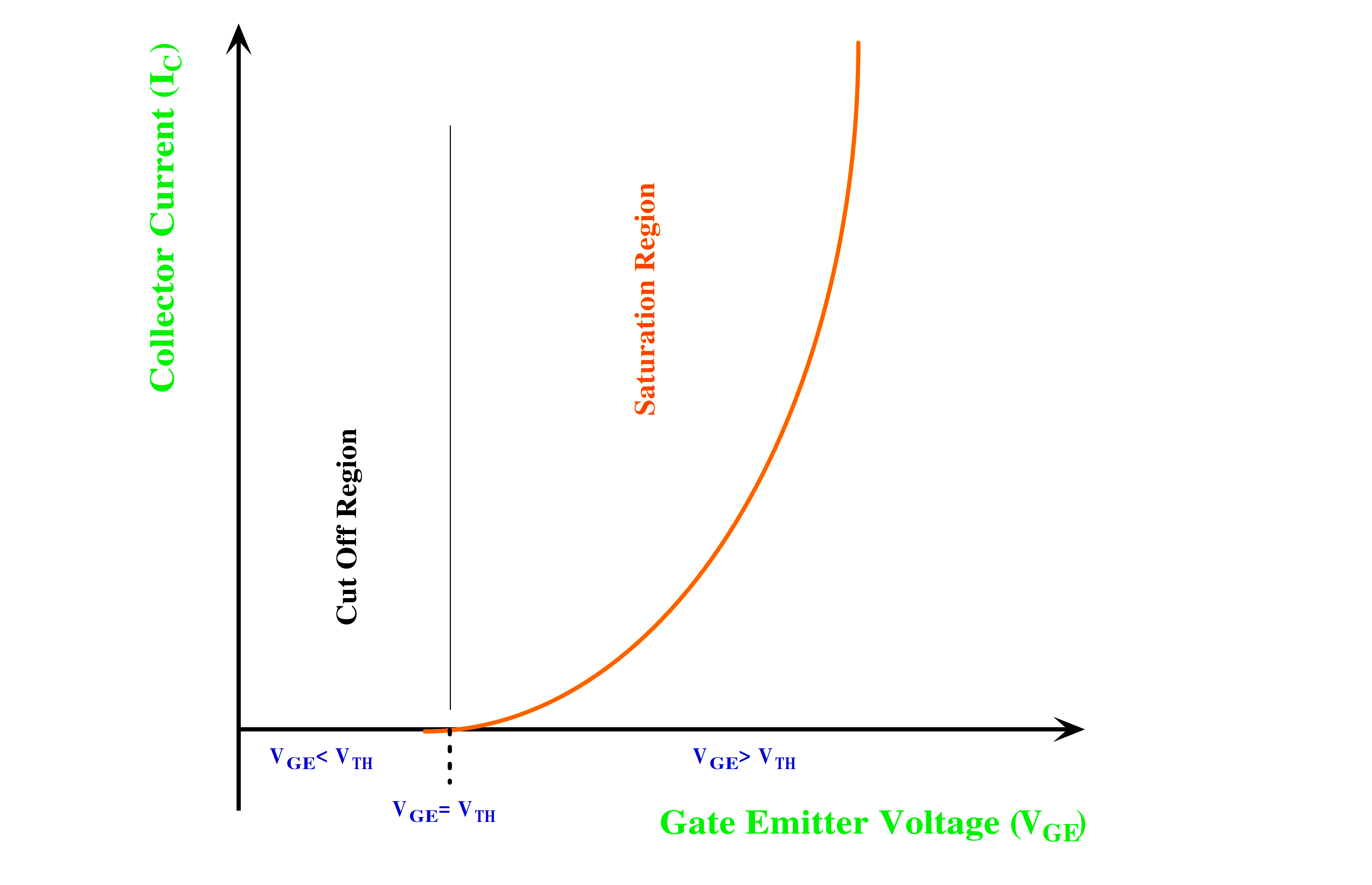
Fig 5. Transfer Characteristics
Output Characteristics
For different values of gate-emitter voltages, the output characteristics are shown between collector current (IC) and collector-emitter voltage (VCE). The output characteristics’ form when moving forward resembles that of a BJT.
IGBTs are voltage-controlled devices, hence in this case the governing parameter is gate emitter voltage VGE. When the device is off, junction J2 blocks forward voltage, and junction J1 prevents reverse voltage if it arises across the collector and emitter.
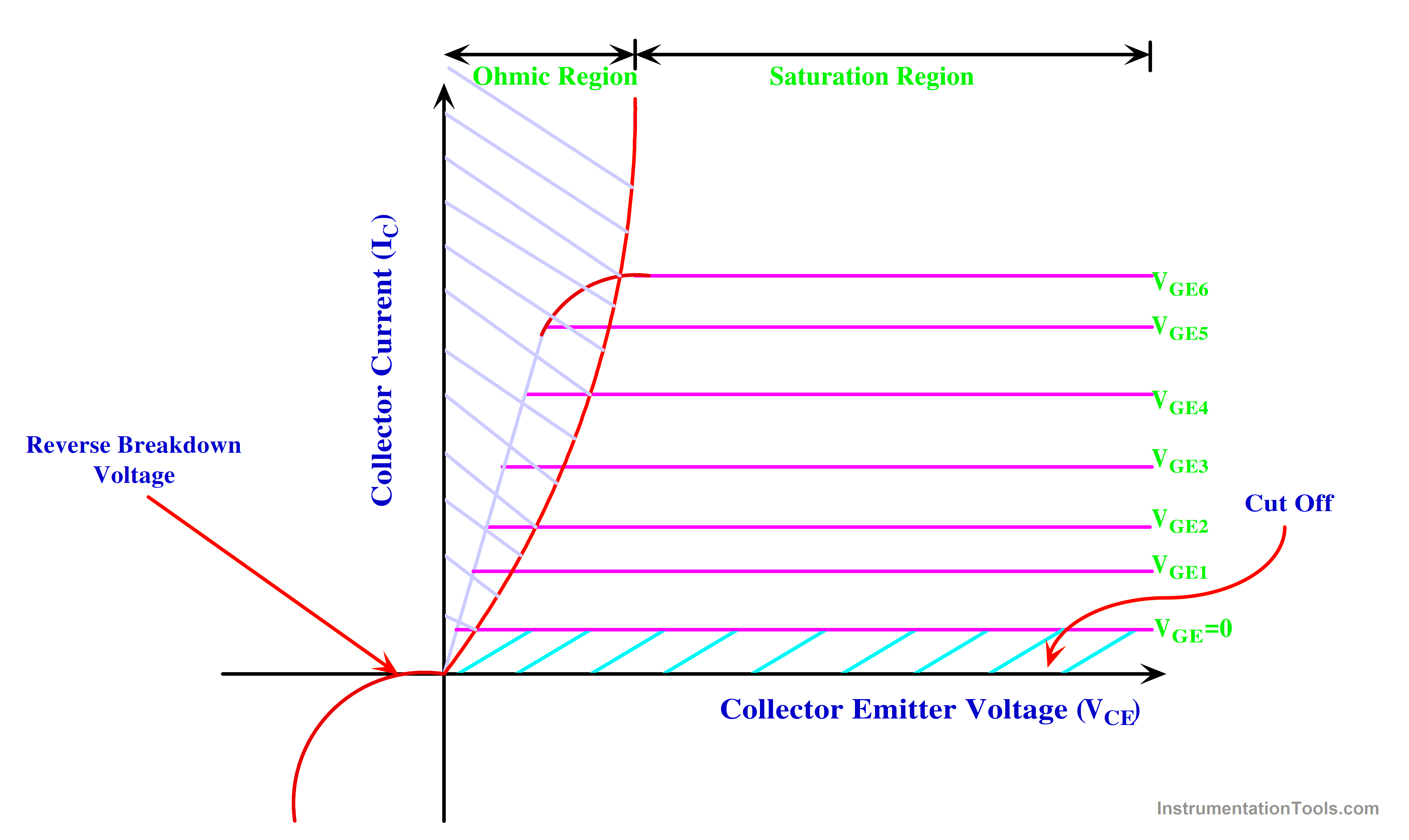
Fig 6. Output Characteristics
Insulated Gate Bipolar Transistor (IGBT) is a semiconductor device used for high-power switching applications in various industries. The switching characteristics of an IGBT are crucial to understanding its behavior during turn-on and turn-off processes.
These characteristics influence the device’s efficiency, power dissipation, and overall performance. Here are some key switching characteristics of IGBTs:
Switching Characteristics of IGBT
Turn on Time
Turn-On Delay Time (tdn): This is the time interval between applying a gate signal and the device’s collector current reaching a certain percentage (usually 10%) of its maximum value. It includes the time taken for the gate voltage to rise, the minority carrier injection into the drift region, and the formation of the conducting channel.
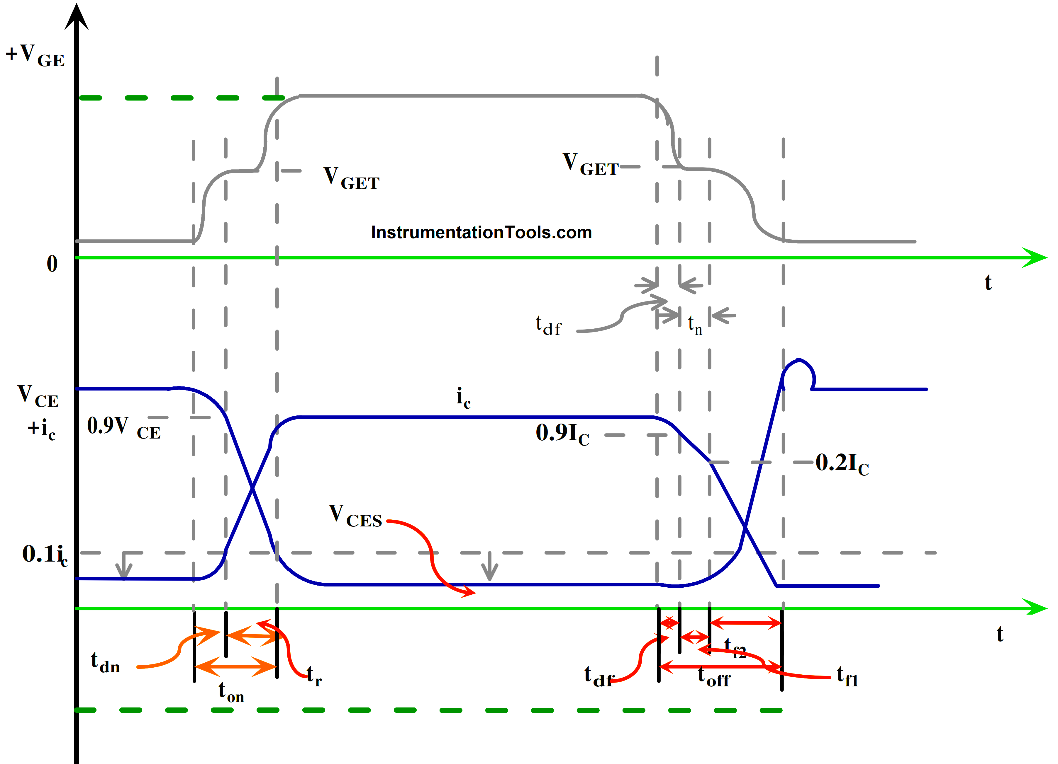
Fig 7 Switching Characteristics
Rise Time (tr): The rise time is the time taken by the collector current to increase from the initial value to a certain percentage (often 90%) of its maximum value. It’s a measure of how quickly the IGBT turns on and starts conducting.
Delay time (tdn) and Rise time (tr) are the two main components of Turn-on time (ton).
Turn OFF Time
Turn-Off Delay Time (tdf): Similar to turn-on delay time, turn-off delay time is the time taken for the collector current to decrease from a certain percentage (usually 90%) of its maximum value to a lower value after the gate signal is removed.
Fall Time or Fall Time 1 (tf1): The fall time is the time taken for the collector current to decrease from a certain percentage (typically 90%) of its maximum value to a lower value during turn-off.
Storage Time or Fall time 2 (tf2): Storage time is the time interval during which the IGBT is transitioning from the on-state to the off-state. It’s the time required for the removal of the excess minority carriers from the drift region.
Switching Energy: Switching energy refers to the energy dissipated during the switching process, including both turn-on and turn-off transitions. Excessive switching energy can lead to higher power losses and reduced efficiency.
Voltage and Current Overshoot: During the switching process, voltage and current spikes can occur due to the device’s parasitic capacitances and inductances. These spikes, if not properly controlled, can cause stress on the device and affect its reliability.
Gate Drive Requirements: The gate drive circuit must provide sufficient voltage and current to ensure quick and efficient switching. Inadequate gate drive can lead to slower switching times, increased power losses, and potential device failure.
Temperature Dependence: The switching characteristics of IGBTs are temperature-dependent. As temperature increases, the switching times might increase, affecting the device’s overall performance.
It’s important to note that the switching characteristics can vary between different IGBT models and manufacturers. Therefore, when designing circuits that use IGBTs, it’s crucial to refer to the device’s datasheet for accurate and detailed information about its switching characteristics under various operating conditions.
Advantages of IGBT
- Minimum Power Loss due to low State Voltage drop
- The Switching frequency of the IGBT is higher than the Power BJT
- The temperature coefficient of resistivity is flat for this material. IGBTS can therefore be connected to one another in parallel.
- Snubber Circuit is not required
Disadvantages of IGBT
- Its blocking power is asymmetric. It is unable to prevent very high reverse voltages.
- Due to the “current tail” included in the turn-off characteristics, excessive power dissipation may occur at the moment of turn-off.
- The switching frequency is not much than MOSFET
Applications of IGBT
- Inverter,
- Choppers,
- SMPS,
- Motor Controller etc
Comparison Between BJT, MOSFET, and IGBT
The below table shows the differences between BJT, MOSFET, and IGBT.
| S. No | BJT | MOSFET | IGBT |
| 1 | BJT is a current controlled device | MOSFET is a voltage-controlled device | IGBT is a voltage-controlled device |
| 2 | The input Impedance of BJT is low. | The input Impedance of MOSFET is high. | The input Impedance of IGBT is low. |
| 3 | The Output Impedance of BJT is low. | The Output Impedance of MOSFET is Medium. | The Output Impedance of IGBT is High. |
| 4 | The temperature coefficient of BJT is negative | The temperature coefficient of MOSFET is positive | The temperature coefficient of IGBT is positive |
| 5 | The maximum switch frequency of a bipolar junction transistor is close to 100KHz | The maximum switching frequency is 300KHz. | Switching frequency up to 50KHz |
| 6 | A BJT has a secondary breakdown limit. | A MOSFET has a safe operating area similar to BJT but does not have a secondary breakdown limit. | No Secondary Breakdown |
| 7 | Poor Thermal Stability used for low power Applications | Poor Thermal Stability | High Thermal Stability |
| 8 | Higher Switching Loss | Lower Switching Loss | Lower Switching loss |
| 9 | On State Voltage drop is High | On State Voltage drop is High | On State Voltage drop is High |
| 10 | Voltage and Current Rating: 1200V to 800A | Voltage and Current Rating: 500V and 140A | Voltage and Current Rating: 1200V and 500A |
Reference
- “Power Electronics: Circuits, Devices and Applications” , M H Rashid, Pearson Education
- “ Power Electronics” P. S. Bimbhra, Khanna Publishers, 2012
- “The MOS controlled thyristor (MCT) as an on-off capacitor bank switch”, Larry Bovino, Sol schneider, John wright.
If you liked this article, then please subscribe to our YouTube Channel for Instrumentation, Electrical, PLC, and SCADA video tutorials.
You can also follow us on Facebook and Twitter to receive daily updates.
Read Next:
- What is Power Electronics?
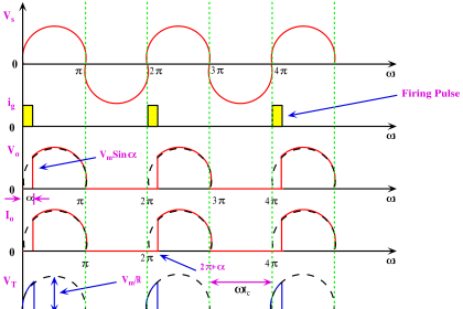
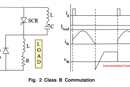
- Turning OFF SCR Commutation
- Types of Power Electronic Devices
- Power Diode Working Principle
- IGBT Characteristics & Advantages