A new kind of thyristor known as an MCT may be closed or opened using control signals. The control energy is comparable to those needed to charge and discharge a power MOSFET’s gate capacitance. The device can be compared to a traditional thyristor in which a MOS gate allows the resistance of the emitter shorts to be adjusted. A traditional or Gate Turn-Off (GTO) thyristor of equal size cannot handle more power than the MCT construction can.
MCT (MOS Controlled Thyristor)
The maximum blocking voltages and controlled currents of MCTs are currently 500 V and 100 A, respectively. In capacitive pulser circuits with both resistive and inductive loads, we have evaluated MCTs as output on-off switches.
Operating the devices in series resulted in significant voltages of up to 1.5k V.
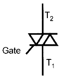
Symbol of MCT
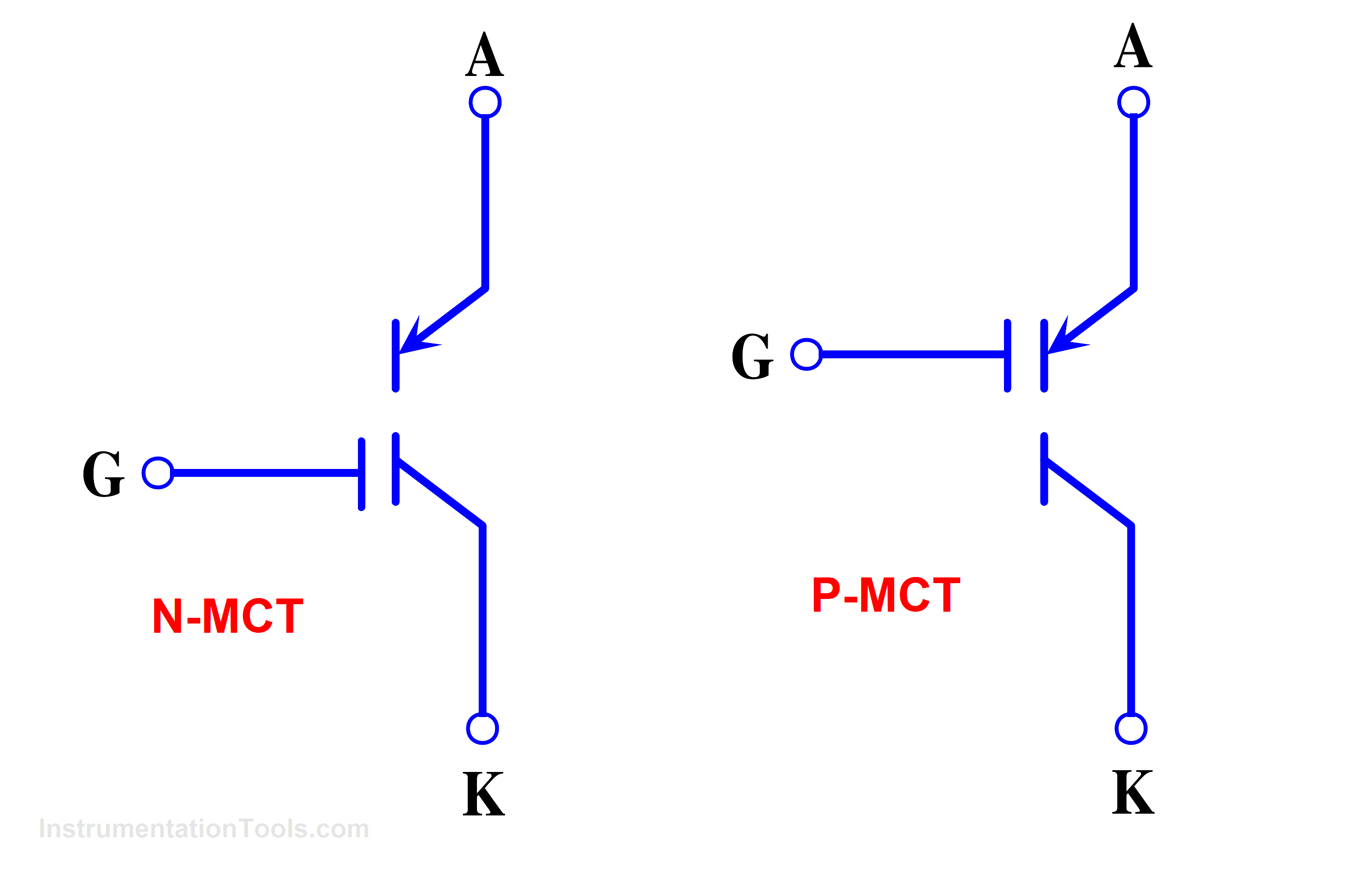
Fig 1. Symbol of MCT
The MCT has the potential to be significant in the field of pulse power due to its capability to repeatedly interrupt current without the need for commutation circuitry and power control circuits.
The device can be compared to a standard thyristor in which a MOS gate allows the resistance of the emitter terminal to be adjusted. The resultant device combines the capacity to handle large amounts of power with minimal conduction loss of a thyristor with the simplicity of turning it off.
Structure of an MCT (MOS Controlled Thyristor)
A MOS gate structure and a standard four-layer thyristor with regenerative activity are both combined into an MCT. But in MCT, the anode serves as the reference to which all gate signals are applied. The reference terminal for gate signals in a traditional SCR is the cathode.
An N-channel MOSFET (M2) and a P-channel MOSFET (M1) comprise the equivalent diagram. The NPNP structure of the MCT is represented by two transistors, NPN (Q1) and PNP (Q2). The analogous circuit’s two transistors show that the MCT provides regenerative feedback just like a normal thyristor.
The N channel MOSFET (M1), connected across the transistor’s emitter and collector (Q2), helps in turning on the MCT, while the P channel MOSFET (M2), connected across the transistor’s emitter and base (Q1), helps in turning it off.
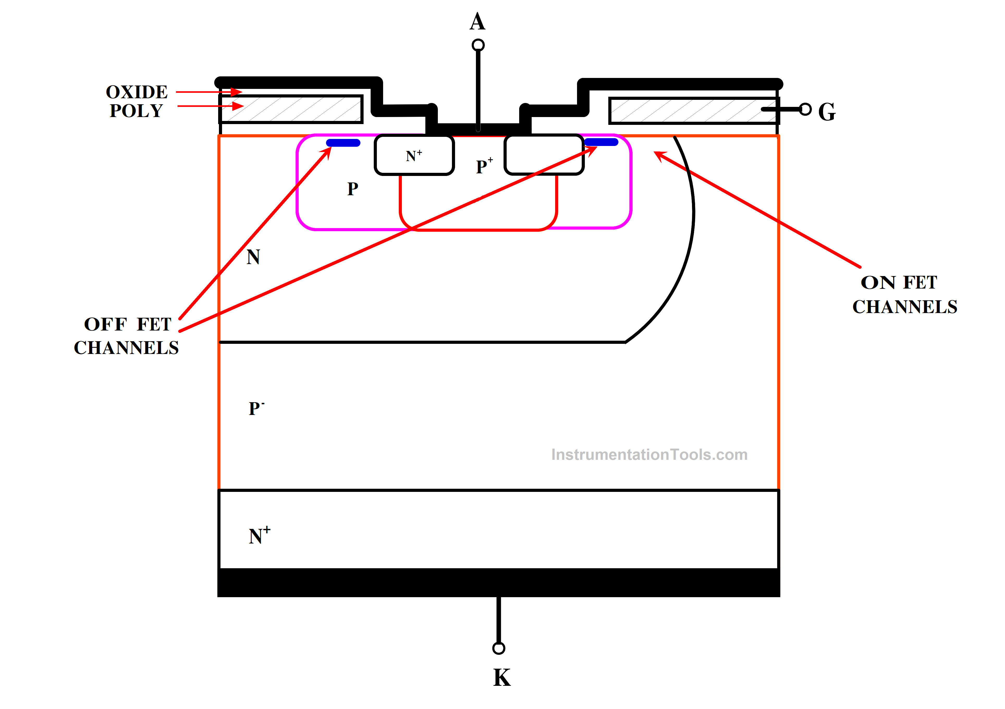
Fig 2. Structure Diagram of MCT
A typical device cross-section of an MCT unit cell with both on- and OFF-FET is shown in Fig 2. Our MCTs only have ON-FET in roughly 4% of the cells, and the cross-section demonstrates that just one gate terminal is needed to operate both FETs.
Working of MCT (MOS Controlled Thyristor)
The MOS control thyristor’s corresponding circuit is depicted in the circuit schematic below. Two MOSFET transistors One N-channel and the other P-channel make up the circuit.
The ON FET switch is activated using the P-channel, while the OFF FET switch is deactivated using the N channel. Two transistors, n-p-n and p-n-p transistors, make up the circuit. If these two transistors are connected together, the MOS control thyristor will have the n-p-n-p structure.
An arrow attached to the gate terminal designates the P channel MOSFET.
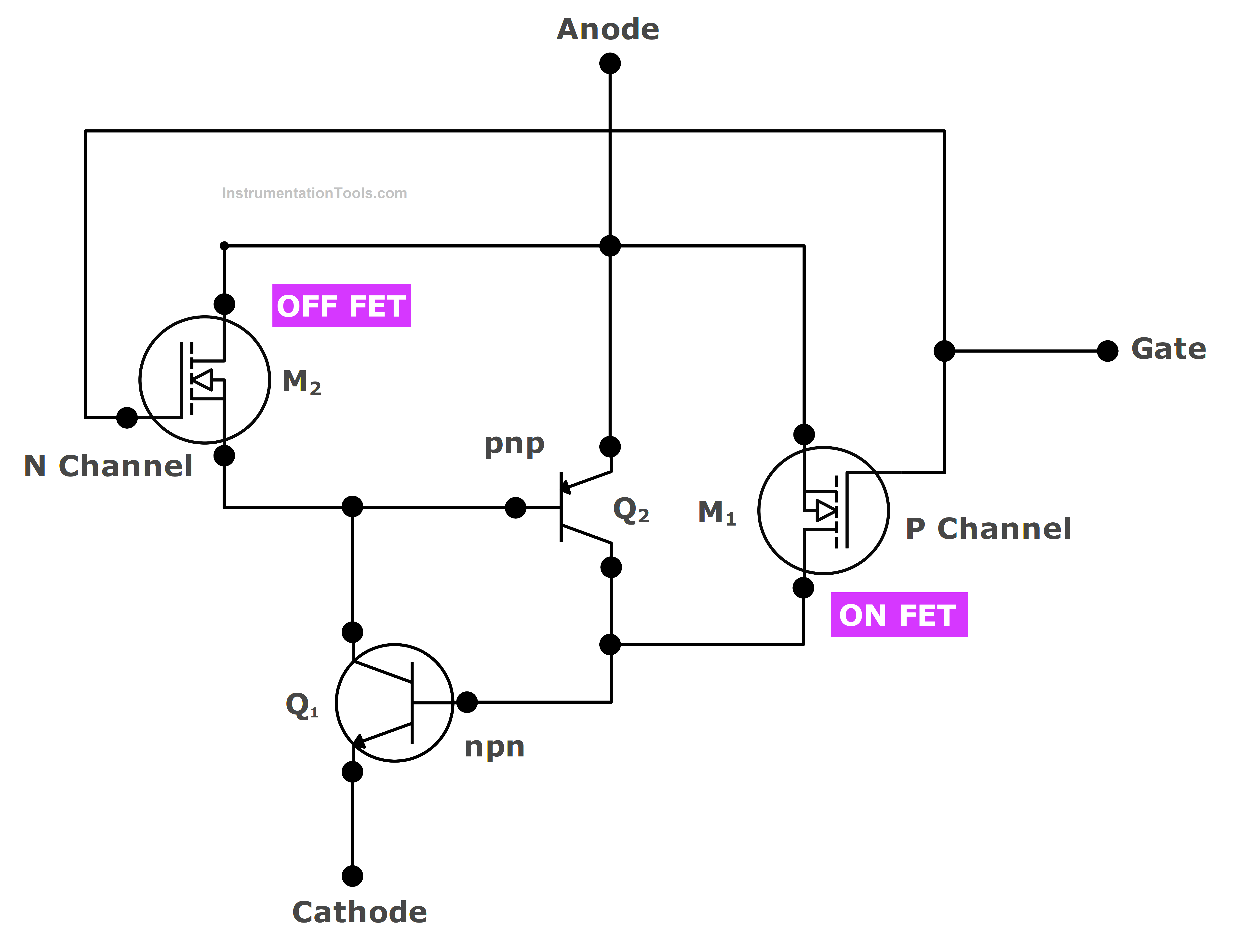
Fig 3. Equivalent Circuit of MCT
A negative voltage pulse at the gate with respect to the anode turns on an MCT, and a positive voltage pulse turns it off.
Turn ON Process
The on-FET must be closed in order to turn on the MCT, but the OFF-FET must be left open. As a result, the lower (Wide base) transistor receives base drive from the externally provided anode-cathode voltage, Vk, which in turn drives the higher (narrow base) transistor.
The MCT latches on and the base drives continue to rise until the device is completely on, just like any thyristor does when enough base drive is available and the total of the transistor gains is more than 1. Currently, the thyristor’s forward voltage drop is about equivalent to that of a single forward-biased p-n junction.
Turn OFF Process
The most intriguing aspect of the MCT is its capacity to shut off, yet the shut-off procedure is relatively straightforward. The condition of the ON-FET is no longer important and may thus be ignored once the thyristor has been latching. By closing the OFF-FET gate, turn-off is achieved.
This essentially disables the higher transistor by shorting the base-emitter junction of the narrow base transistor. The wide-base transistor loses base drive as a result and starts to switch off. Carrier recombination in the broad base is therefore primarily responsible for the MCT anode current fall-time.
During turn-off, the OFF-FET is required to temporarily run at full anode current. The OFF-FET must thus be constructed in a way that minimizes the drain to source ON resistance, Rd on. The quantity of off-FET channels and their Rd on govern the turn-off capabilities of the MCT.
The FET does not need to have a very high voltage blocking capacity, which allows Rd on to be manufactured extremely tiny. The diode drops of the narrow base transistor’s forward-biased base-emitter junction, which is typically less than 1 V, is the greatest voltage that the OFF-FET would ever experience.
Gate Voltage Requirement of MCT
The gate drive requirements of the MCT can be simply explained in terms of controlling the on- and OFF-FET. The FETs are controlled by a gate signal, V which is referenced to the MCT anode. The MCTs described here have n-channel OFF-FET and p-channel ON-FET.
Both FETs are enhancement mode devices, that is if V = 0, both FETs are open. This condition leaves the MCT susceptible to ‘noise’ or dV /dt turn-on as is the case in any thyristor without emitter shorts. Therefore, maintaining V positive is desirable to bias the MCT off. With the OFF-FET thus held closed, the MCT is virtually immune to dV/dt turn-on.
The Vg is changed to a negative value, the OFF-FET is opened, and the ON-FET is closed to shut the MCT. Returning Vg to a positive level high enough to shut the OFF-FET opens the device. The MCT is turned on and off, respectively, using signal levels of Vg = + 12V and V = -5V. The OFF-FETs is pushed considerably beyond its gate threshold voltage to reduce Rds on and maximize turn-off capabilities. Turning it on is not crucial.
The MCT gate looks like a capacitance. Once charged, it is not load-sensitive and doesn’t need any current. Therefore, the highest gate energy needed to turn the MCT on or off is approximately 1.16 microjou1es from 1/2CV2. At normal temperatures, these devices can shut off up to 100 A. Although its forward repeating surge (pulse) current has not yet been established, it is anticipated to be about 500 A.
To switch the MCT gate in 100 ns requires a peak current of only about 1.36 A, from C dV/dt. In contrast, a Gate Turn-Off thyristor (GTO) requires that 20% to 35% of the anode current be diverted through the gate drive circuit for the entire duration of turn-off depending on the particular GTO, typically 2 to 20 microseconds
VI Characteristics of MCT
The VI Characteristics of MCT is shown in Fig 4. The Anode(A) is made as positive with respect to the cathode(K), The MCT stays in the blocking state when no voltage is supplied to the gate, only permitting a little leakage current (ILEAK).
When a breakover voltage VBO is achieved, the MCT enters a condition of breakdown and doesn’t return to its off state. This method does not, however, activate the MCT.
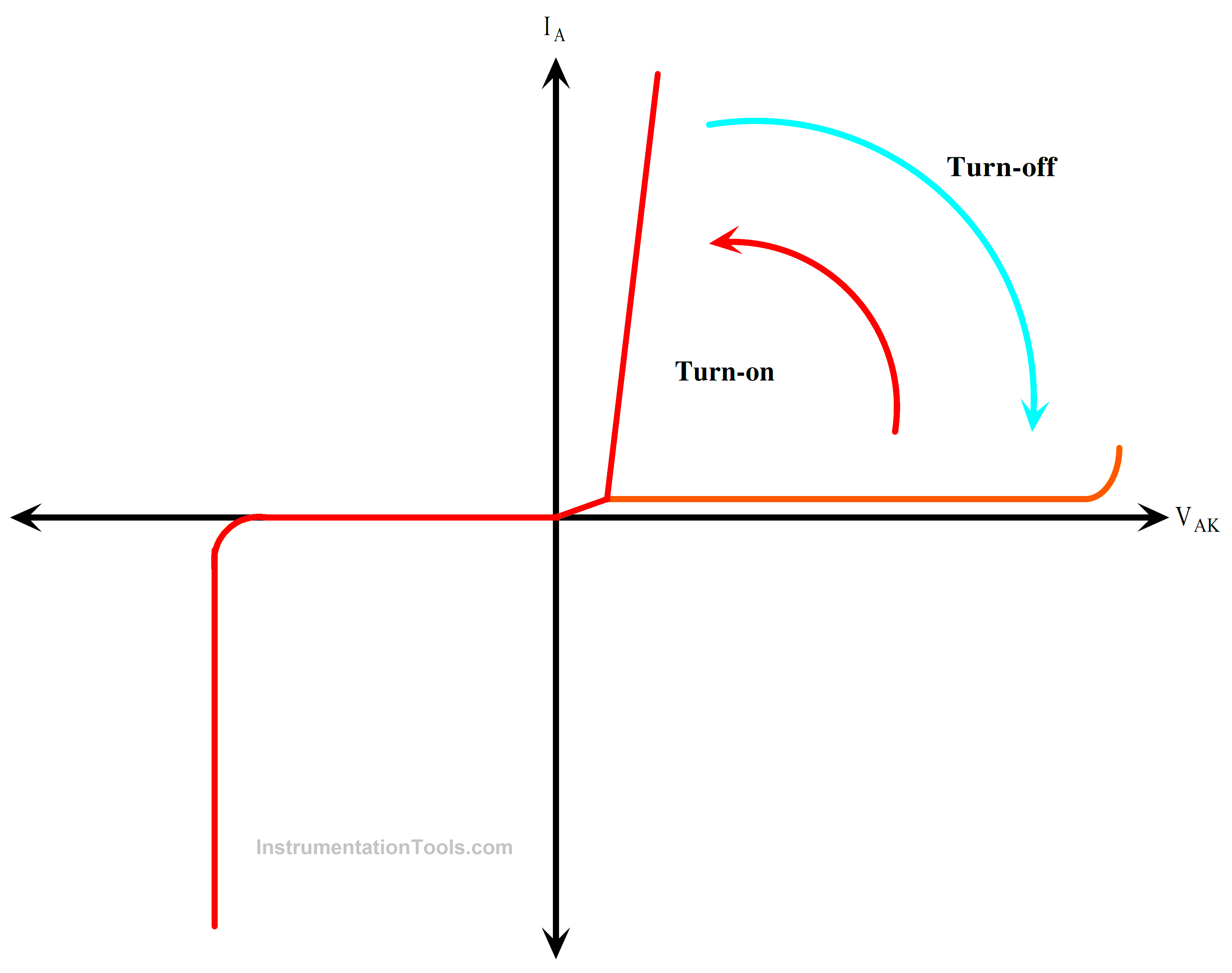
Fig 4. VI Characteristics of MCT
By making the anode positive with respect to the cathode and supplying a negative voltage to the gate and anode, the device is typically turned on by forward biasing the MCT. When the MCT is turned on, the voltage drops across it (VON) is very minimal (approximately 1V), and the load resistance is the only factor limiting the anode current.
If the gate voltage is removed after the MCT goes ON, it will not switch off. When the MCT is turned ON, applying a positive voltage to the gate disables the component until a subsequent negative voltage is supplied to the gate.
Advantages of MCT
- Forward conduction drop is minimal.
- Faster on and off timings.
- Minimal switching losses.
- High gate input impedance makes designing driver circuits simple.
Advantage of MCT over IGBT
- Low forward voltage drop.
- It is anticipated that N-type MCTs would have a comparable forward voltage drop but a better reverse bias safe working area and switching speed.
- The switching and storing periods of MCTs are very short.
- High current densities and blocking voltages in both directions are possible with the MCT.
Disadvantages of MCT
- Required high gate pulse to turn OFF the device
- Low reverse blocking capability
- When a device is turned off at greater current levels, there is a chance that it might be destroyed.
Applications of MCT
- DC to DC converters
- Circuit Breakers
- Induction Heating
- Variable Power Factor applications and much more.
Reference
- “Power Electronics: Circuits, Devices and Applications” , M H Rashid, Pearson Education
- “ Power Electronics” P. S. Bimbhra, Khanna Publishers, 2012
- “The MOS controlled thyristor (MCT) as an on-off capacitor bank switch”, Larry Bovino, Sol schneider, John wright.
If you liked this article, then please subscribe to our YouTube Channel for Instrumentation, Electrical, PLC, and SCADA video tutorials.
You can also follow us on Facebook and Twitter to receive daily updates.
Read Next:
- What is Power Electronics?
- Power MOSFET Advantages
- Types of Power Electronic Devices
- Power Diode Characteristics
- IGBT Characteristics & Advantages