What is CPLD?
CPLDs, or complex programmable logic devices, fulfill their promises in full. In essence, they are made to mimic multiple PALs that have been combined into a single chip and are interconnected by a crosspoint switch. Since they are based on the same technology, employ the same programmers, and use the same development tools, they can manage higher volume and complexity of reasoning.
Although the FPGA and SPLD are more advanced than the CPLD (complex programmable logic device), they function similarly to the CPLD. CPLDs are more complicated than SPLDs but less complex than FPGAs. The PAL (programmable array logic), PLA (programmable logic array), and GAL are the most often utilized SPLDs (generic array logic).
What is FPGA?
Field programmable gate arrays (FPGAs), a semiconductor device, have a customizable logic block (CLB) matrix that is connected by programmable interconnects. After being manufactured, an FPGA board can be reprogrammed to meet specific application or feature requirements.
FPGA chips are distinguished from Application-Specific Integrated Circuits (ASICs), which are developed especially for certain design requirements, by this feature. SRAM-based FPGAs, which can be updated as the design changes, are more popular than one-time programmable (OTP) FPGA development boards.
Field Programmable Gate Arrays are structured very much like gate array ASICs, not like PALs or other programmable devices. The use of FPGAs in ASIC prototypes and other situations where an ASIC will eventually be used.
CPLD Architecture
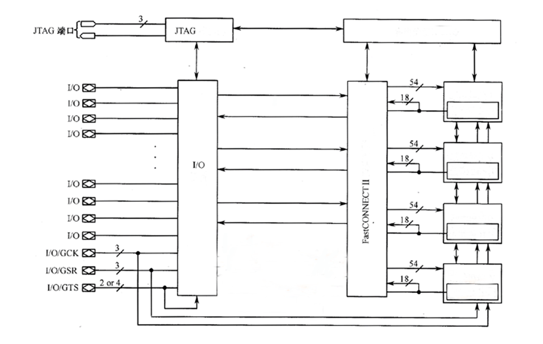
The CPLD is composed of many PAL structures known as macrocells and is a development of PAL. Every input pin in the CPLD package is accessible to every macrocell, but each macrocell only has one output pin. The block diagram of a CPLD can be seen in the accompanying image.
The block diagram makes clear that a CPLD is composed of numerous macrocells or function blocks. The macrocells (global interconnection matrix) are connected via a programmable interconnect, also referred to as GIM. Rearranging the GIM enables the construction of several logic circuits. Digital I/Os are used by CPLDs to interface with external hardware.
CPLD Structure
The basic structure of CPLD is introduced using the Xilinx XC9500XL series chip as an example. The structure of CPLD is based on the product term (Product-Term). The Function Block, FastCONNECT II SwitchMatrix, and I/O control module are the three components that make up the CPLD. The graphic depicts the construction of each function block, which is made up of a programmable array, a product term allocator, and 18 macrocells.
The I/O control module is in charge of setting open collector outputs, tri-state outputs, and other electrical properties of the input outputs. The global clock, global reset, and global output enable signals are I/O/GCK, I/O/GSR, and 1/0/GTS, respectively, and are connected to each function module in the CPLD with a specific line.
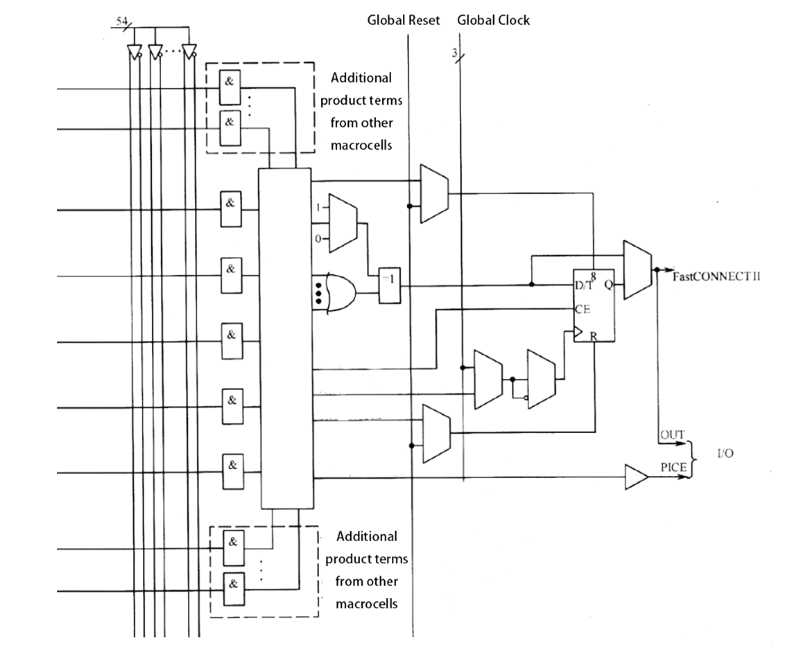
The macro cell, which is a core part of the CPLD, executes the basic logic operations. The macro cell’s basic structure is depicted in the image below. A product term array, which is actually an array with or without, is shown on the left side of the image.
Each cross-point is programmable, and if it is turned on, it realizes the “with” logic and completes the combination logic alongside the product term allocator in the background. Its clock and clear inputs can be programmed to use a separate global clear and global clock or to utilize the clock and clear generated by the internal logic (product term array).
The programmable flip-flop on the right side of the image can be configured as a D flip-flop or a T flip-flop. If the trigger is not required, it can alternatively be disregarded and the signal sent to the I/0 pin or the connection matrix.
CPLD Components
CPLD Components include programmable components, function block, interconnect, and input/Output blocks. You can see the below detailed description between them.
Programmable Components: Additionally, it makes use of programmable parts like flash EPROM, EEPROM, PROM, and ROM.
Function block: A function block in a CPLD features an AND plane that can take inputs from I/O blocks, function blocks, or even the response of the same function block. The terms are then selected using a large multiplexer after being added to the OR array.
Either directly or through a timed flip-flop, the output of the MUX can be relocated from the block. This functional block may additionally have extra logic, such as a master reset signal, a selectable exclusive OR, and the ability to program the polarity in stages.
Interconnect: A CPLD’s interconnect is a sizable matrix of programmable switches that controls how signals are transferred from one area of the device to another.
Input/Output blocks: Signals are sent to the CPLD pins using the input/output blocks at the correct voltage and current levels. It enables the elimination of delays, a reduction in the amount of time the device must be held idle, and the addition of more resources to the device.
Pros of CPLD
- It’s simple to design.
- It was developed at a modest cost.
- CPLD helps to make the board smaller.
- High reliability is provided by it.
Cons of CPLD
- A more advanced programmable logic device than an SPLD is a CPLD.
- It is a more intricate piece of programmable logic.
How does CPLD work?
Utilizing CMOS EPROM, EEPROM, flash memory, and SRAM programming technologies, CPLD creates incredibly dense, fast, and energy-efficient programmable logic devices. They belong to the class of large-scale integrated circuits and have relatively complex structures and a huge size. A CPLD is a kind of digital integrated circuit that enables users to create unique logic circuits based on their own requirements.
The main approach to design is to implement the planned digital system using the integrated development software platform and hardware description language, transfer the code to the target chip via the download cable (referred to as “in-system” programming), and then produce the matching target file.
FPGA Architecture
Three different types of modules are used in the fundamental FPGA design. These are made up of I/O blocks or pads (CLB), connector lines, switch matrices, and programmable logic blocks (CLB). A user can link two-dimensional arrays of logic blocks in any sequence to create the fundamental FPGA design. This article discusses the functions of an FPGA architectural module.
A CLB (Configurable Logic Block) is a unit of logic and digital inputs and outputs. It carries out user logic. The interconnects provide instructions to the logic blocks so they can execute user logic. The switch matrix provides logic-based connection switching. I/O pads are used to link many applications to the outside world.
FPGA Basics
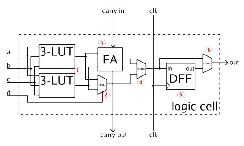
A single CLB is made up of several logic blocks (see image below). An FPGA’s lookup table (LUT) is one of its distinguishing characteristics. For any combination of inputs, a LUT holds a predetermined list of logic outputs; LUTs with four to six input bits are typical. Popular logic operations include flip-flops, full adders, and multiplexers.
The CLB’s components vary depending on the device in terms of number and configuration; the simplified version in Figure 2 has two three-input LUTs (1), an FA (3), a D-type flip-flop (5), as well as a regular mux (2) and two muxes that are programmed into the FPGA.
There are two ways that the condensed CLB can function. The inputs to the FA in arithmetic mode consist of the LUT outputs and a carry input from another CLB. The LUTs and Mux 2 are connected in normal mode to create a four-input LUT. Mux 4 decides whether to use the FA output or the LUT output. Using the D flip-flop, Mux 6 determines whether an operation is asynchronous or synchronized to the FPGA clock.
The more advanced CLBs found in current-generation FPGAs may do many operations with only one block and can be coupled to execute more complicated operations like multipliers, registers, counters, and even digital signal processing (DSP) activities.
FPGA Components
- The I/O Block is used to connect chips.
- Using programmable routing makes it possible to use functions.
- Logic functions can be implemented using programmable logic blocks.
Pros of FPGA
- FPGA development is less expensive than ASIC development because there are no NRE (Non-Recurring Expenses) and less expensive tools are used.
- FPGAs are always programmable at the software level. The FPGA IC may thus be reconfigured or reused indefinitely. FPGAs can also be remotely programmed.
- With HDL code, FPGA ICs may be easily programmed and are widely available. The consequence is a quicker release of the solution to the market.
- Routing, placement, and timing are handled by software in FPGA design. It necessitates less manual labor. Time-consuming and difficult place and router, floor planning, and timing considerations are eliminated by the design flow.
- FPGAs have the capability of logic-level programming. As a result, it might use more parallel and quicker signal processing. Execution by the CPU is difficult.
Cons of FPGA
- Basic knowledge of digital systems and the VHDL/Verilog programming languages are prerequisites for programming FPGAs. The programming is more complex than that used in equipment with processors. Additionally, engineers must understand how to use simulation software.
- The size and characteristics of the design are constrained by the resources available on the FPGA IC once it has been selected and used in the design. In order to prevent this issue, a suitable FPGA must be chosen from the beginning.
- The FPGA has increased power consumption, and programmers have little control over power optimization.
- Prototyping and low-volume production work well with FPGAs. The cost per unit likewise grows as the number of FPGAs to be produced does.
How does FPGA work?
FPGAs are within the family of devices known as programmable logic, also referred to as programmable hardware. Although it doesn’t actually do anything on its own, an FPGA may be programmed to be practically any digital circuit you choose. This condition is magical since nothing actually changes.
Simply loading a configuration onto the FPGA will cause it to start acting like the desired circuit. Soldering, jumper wires, and hassle are not necessary. An FPGA can then be altered to behave like yet another circuit, and still another, and yet another. The arrangement can essentially be modified as often as necessary because it is RAM-based.
Even while we describe building digital circuits using FPGAs, you don’t typically create designs for them by sketching diagrams. The size and complexity of the circuits that FPGAs may contain would make it challenging to develop a schematic. Instead, by describing the desired behavior, you can use the tools to create a circuit that matches the behavior of the circuit you want.
CPLD Applications
- Complex programmable logic circuits are ideal for high-performance, demanding control applications.
- CPLDs can be used in digital designs to perform bootloader functions.
- Field programmable gate array configuration data are loaded from non-volatile memory using CPLD technology.
- They are typically employed for straightforward design operations like address decoding.
- Due to their small size and low power consumption, CPLDs are often employed in a variety of applications, such as in price-sensitive, battery-operated portable devices.
FPGA Applications
FPGAs have soared in popularity over the past ten years thanks to their versatility in a variety of applications. A few applications that use an FPGA specifically include voice recognition, cryptography, filtering, communication encoding, device controllers, software-defined radio, random logic, ASIC prototyping, medical imaging, computer hardware emulation, and device controllers.
The majority of vertical applications for FPGAs are specialized, low-volume ones. The best companies spend on the hardware expenses per unit for these low-volume applications. The number of practical applications has now risen as a result of the better performance dynamics and cost.
FPGA vs. CPLD
| FPGA | CPLD |
| FPGAs, on the other hand, are short for field programmable gate arrays. | CPLDs stand for Complex Programmable Logic Devices. |
| On top of RAM is a digital logic chip called an FPGA. | Contrarily, CPLDs are EEPROM-based. |
| CPLD delays are far more predictable than FPGA delays. | Because CPLD has nonvolatile memory, it is more secure than FPGA. |
| The category of fine grain includes FPGA. | Contrarily, CPLD is of the coarse grain variety. |
| A Gate array and FPGA are comparable. | The CPLD, however, is the PAL’s counterpart. |
| Internal routing is dependable since it has little impact on FPGA performance. | On the other hand, the CPLD’s performance varies and is reliant on routing. |
| FPGA consumes more power. | In comparison, the CPLD has a reduced power usage. |
| FPGA is a good fit for complex apps. | However, the CPLD operates more well in simpler applications. |
| An FPGA has up to 100,000 small logic blocks. | CPLDs, in contrast, can only hold a small number of thousand logic blocks. |
| As opposed to this, an FPGA is a type of integrated circuit that is primarily made to be altered by a client or a developer after it is made. | A digital system’s operation is helped by a CPLD integrated circuit. |
The conclusion between CPLD and FPGA
The transition from discrete logic devices to entry-level FPGAs is made possible by simple programmable logic devices (SPLDs) and complex programmable logic devices (CPLDs), which are less complex components. Low power consumption, low logic density, and minimal complexity per chip are the main features of entry-level FPGAs.
Functional blocks with specific functions are added by devices with expanded functionality: Phase-locked loops (PLLs), high-speed serializers, and deserializes are a few examples, as are high-speed transceivers, Ethernet MACs, PCI Express controllers, and high-speed serializers. Either solo circuits (hard IP) or CLBs (soft IP) can be created utilizing these building blocks. Performance is increased by hard IP blocks at the expense of reconfigurability.
The most sophisticated system-on-chip (SoC) components for the FPGA product family combine a microprocessor CPU core, hard IP, and the FPGA architecture into a single device. When compared to standalone devices, a SoC FPGA offers more integration, lower power consumption, a smaller board footprint, and higher-bandwidth communication between the core and extra blocks.