Inst ToolsInst ToolsInst Tools
  • Courses
  • Automation
    • PLC
    • Control System
    • Safety System
    • Communication
    • Fire & Gas System
  • Instrumentation
    • Design
    • Pressure
    • Temperature
    • Flow
    • Level
    • Vibration
    • Analyzer
    • Control Valve
    • Switch
    • Calibration
    • Erection & Commissioning
  • Interview
    • Instrumentation
    • Electrical
    • Electronics
    • Practical
  • Q&A
    • Instrumentation
    • Control System
    • Electrical
    • Electronics
    • Analog Electronics
    • Digital Electronics
    • Power Electronics
    • Microprocessor
  • Request
Search
  • Books
  • Software
  • Projects
  • Process
  • Tools
  • Basics
  • Formula
  • Power Plant
  • Root Cause Analysis
  • Electrical Basics
  • Animation
  • Standards
  • 4-20 mA Course
  • Siemens PLC Course
Reading: N Type and P Type Semiconductors
Share
Notification Show More
Font ResizerAa
Inst ToolsInst Tools
Font ResizerAa
  • Courses
  • Design
  • PLC
  • Interview
  • Control System
Search
  • Courses
  • Automation
    • PLC
    • Control System
    • Safety System
    • Communication
    • Fire & Gas System
  • Instrumentation
    • Design
    • Pressure
    • Temperature
    • Flow
    • Level
    • Vibration
    • Analyzer
    • Control Valve
    • Switch
    • Calibration
    • Erection & Commissioning
  • Interview
    • Instrumentation
    • Electrical
    • Electronics
    • Practical
  • Q&A
    • Instrumentation
    • Control System
    • Electrical
    • Electronics
    • Analog Electronics
    • Digital Electronics
    • Power Electronics
    • Microprocessor
  • Request
Follow US
All rights reserved. Reproduction in whole or in part without written permission is prohibited.
Inst Tools > Blog > Electronic Devices & Circuits > N Type and P Type Semiconductors

N Type and P Type Semiconductors

Last updated: October 5, 2016 1:25 pm
Editorial Staff
Electronic Devices & Circuits
No Comments
Share
5 Min Read
SHARE

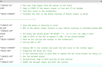
Semiconductive materials do not conduct current well and are of limited value in their intrinsic state. This is because of the limited number of free electrons in the conduction band and holes in the valence band. Intrinsic silicon (or germanium) must be modified by increasing the number of free electrons or holes to increase its conductivity and make it useful in electronic devices. This is done by adding impurities to the intrinsic material. Two types of extrinsic (impure) semiconductive materials, n-type and p-type, are the key building blocks for most types of electronic devices.

Since semiconductors are generally poor conductors, their conductivity can be drastically increased by the controlled addition of impurities to the intrinsic (pure) P. This process, called doping, increases the number of current carriers (electrons or holes). The two categories of impurities are n-type and p-type.

N-Type Semiconductor

To increase the number of conduction-band electrons in intrinsic silicon, pentavalent impurity atoms are added. These are atoms with five valence electrons such as arsenic (As), phosphorus (P), bismuth (Bi), and antimony (Sb).

As illustrated in Below Figure, each pentavalent atom (antimony, in this case) forms covalent bonds with four adjacent silicon atoms. Four of the antimony atom’s valence electrons are used to form the covalent bonds with silicon atoms, leaving one extra electron. This extra electron becomes a conduction electron because it is not involved in bonding. Because the pentavalent atom gives up an electron, it is often called a donor atom. The number of conduction electrons can be carefully controlled by the number of impurity atoms added to the silicon. A conduction electron created by this doping process does not leave a hole in the valence band because it is in excess of the number required to fill the valence band.

n-type-semiconductor

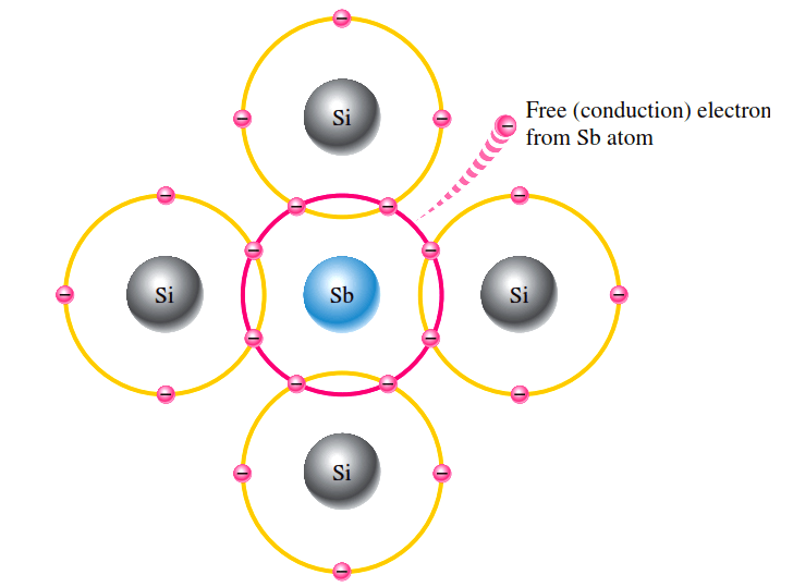
Fig: Pentavalent impurity atom in a silicon crystal structure. An antimony (Sb) impurity atom is shown in the center. The extra electron from the Sb atom becomes a free electron.

Majority and Minority Carriers Since most of the current carriers are electrons, silicon (or germanium) doped with pentavalent atoms is an n-type semiconductor (the n stands for the negative charge on an electron). The electrons are called the majority carriers in n-type material. Although the majority of current carriers in n-type material are electrons, there are also a few holes that are created when electron-hole pairs are thermally generated. These holes are not produced by the addition of the pentavalent impurity atoms. Holes in an n-type material are called minority carriers.

P-Type Semiconductor

To increase the number of holes in intrinsic silicon, trivalent impurity atoms are added. These are atoms with three valence electrons such as boron (B), indium (In), and gallium (Ga). As illustrated in Below Figure, each trivalent atom (boron, in this case) forms covalent bonds with four adjacent silicon atoms. All three of the boron atom’s valence electrons are used in the covalent bonds; and, since four electrons are required, a hole results when each trivalent atom is added. Because the trivalent atom can take an electron, it is often referred to as an acceptor atom. The number of holes can be carefully controlled by the number of trivalent impurity atoms added to the silicon. A hole created by this doping process is not accompanied by a conduction (free) electron.

p-type-semiconductor

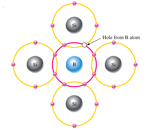
Fig: Trivalent impurity atom in a silicon crystal structure. A boron (B) impurity atom is shown in the center.

Majority and Minority Carriers Since most of the current carriers are holes, silicon (or germanium) doped with trivalent atoms is called a p-type semiconductor. The holes are the majority carriers in p-type material. Although the majority of current carriers in p-type material are holes, there are also a few conduction-band electrons that are created when electron-hole pairs are thermally generated. These conduction-band electrons are not produced by the addition of the trivalent impurity atoms. Conduction-band electrons in p-type material are the minority carriers.

Don't Miss Our Updates
Be the first to get exclusive content straight to your email.
We promise not to spam you. You can unsubscribe at any time.
Invalid email address
You've successfully subscribed !

Continue Reading

Power MOSFET Safe Operating Area
Comparison of Half wave Rectifiers and Full wave Rectifiers
Diode Clampers Principle
Schottky Diode Working Principle
Ripple Voltage in Rectifiers
Transistor as an Amplifier in Common Emitter
Share This Article
Facebook Whatsapp Whatsapp LinkedIn Copy Link
Share
Leave a Comment

Leave a Reply Cancel reply

Your email address will not be published. Required fields are marked *

Stay Connected

128.3kFollowersLike
69.1kFollowersFollow
210kSubscribersSubscribe
38kFollowersFollow

Categories

Explore More

Characteristics of Photo diode
Troubleshooting a Biased Transistor
Transistor Cut off, Saturation & Active Regions
Time Base Generator
Half Wave Voltage Doubler using Diodes
Transistor Load Line Analysis
Diodes Voltage Quadrupler
Shockley Diode Working Principle

Keep Learning

Diode-positive-limiter

Positive & Negative Diode Clippers

Types-of-diodes

Different Types of Diodes

Schottky Diode Vs PN junction Diode

Difference between Schottky Diode and PN junction Diode

phototransistor symbols

Phototransistor Working Principle

Transistor as Amplifier

Transistor as Amplifier

Transistor Collector Characteristic Curves

Transistor Collector Characteristic Curves

Capacitor Filter Operation

Capacitor Filter Operation

Zener Diode Voltage Regulator Operation

Zener Diode Voltage Regulator Operation

Learn More

Control Valve pressure recovery

What is Control Valve Flashing ?

Redundant Power Supply WITH Diode Unit

Redundant Power Supply for Critical Field Panels

Single-Phase Induction Motors Multiple Choice Questions (MCQ)

125+ Single-Phase Induction Motors Multiple Choice Questions (MCQ)

P&ID Guidelines for Storage Tanks

P&ID Guidelines for Storage Tanks

Types of Failures in Control Valves

Types of Failures in Control Valves

Weight-based Level Instruments Principle

Weight-based Level Measurement Principle

What is an RTD

Components of RTD

PLC Logic for Water Pumping and Chemical Addition

Developing PLC Logic for Water Pumping and Chemical Addition

Menu

  • About
  • Privacy Policy
  • Copyright

Quick Links

  • Learn PLC
  • Helping Hand
  • Part Time Job

YouTube Subscribe

Follow US
All rights reserved. Reproduction in whole or in part without written permission is prohibited.
Welcome Back!

Sign in to your account

Username or Email Address
Password

Lost your password?