Inst ToolsInst ToolsInst Tools
  • Courses
  • Automation
    • PLC
    • Control System
    • Safety System
    • Communication
    • Fire & Gas System
  • Instrumentation
    • Design
    • Pressure
    • Temperature
    • Flow
    • Level
    • Vibration
    • Analyzer
    • Control Valve
    • Switch
    • Calibration
    • Erection & Commissioning
  • Interview
    • Instrumentation
    • Electrical
    • Electronics
    • Practical
  • Q&A
    • Instrumentation
    • Control System
    • Electrical
    • Electronics
    • Analog Electronics
    • Digital Electronics
    • Power Electronics
    • Microprocessor
  • Request
Search
  • Books
  • Software
  • Projects
  • Process
  • Tools
  • Basics
  • Formula
  • Power Plant
  • Root Cause Analysis
  • Electrical Basics
  • Animation
  • Standards
  • 4-20 mA Course
  • Siemens PLC Course
Reading: Transistor Collector Characteristic Curves
Share
Notification Show More
Font ResizerAa
Inst ToolsInst Tools
Font ResizerAa
  • Courses
  • Design
  • PLC
  • Interview
  • Control System
Search
  • Courses
  • Automation
    • PLC
    • Control System
    • Safety System
    • Communication
    • Fire & Gas System
  • Instrumentation
    • Design
    • Pressure
    • Temperature
    • Flow
    • Level
    • Vibration
    • Analyzer
    • Control Valve
    • Switch
    • Calibration
    • Erection & Commissioning
  • Interview
    • Instrumentation
    • Electrical
    • Electronics
    • Practical
  • Q&A
    • Instrumentation
    • Control System
    • Electrical
    • Electronics
    • Analog Electronics
    • Digital Electronics
    • Power Electronics
    • Microprocessor
  • Request
Follow US
All rights reserved. Reproduction in whole or in part without written permission is prohibited.
Inst Tools > Blog > Electronic Devices & Circuits > Transistor Collector Characteristic Curves

Transistor Collector Characteristic Curves

Last updated: September 27, 2016 2:28 pm
Editorial Staff
Electronic Devices & Circuits
No Comments
Share
3 Min Read
SHARE

Using a circuit like that shown in Figure (a), a set of collector characteristic curves can be generated that show how the collector current, IC, varies with the collector-to-emitter voltage, VCE, for specified values of base current, IB. Notice in the circuit diagram that both VBB and VCC are variable sources of voltage.

Transistor Collector Characteristic Curves

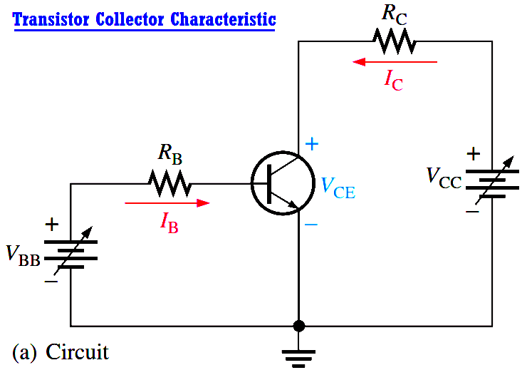
Assume that VBB is set to produce a certain value of IB and VCC is zero. For this condition, both the base-emitter junction and the base-collector junction are forward-biased because the base is at approximately 0.7 V while the emitter and the collector are at 0 V. The base current is through the base-emitter junction because of the low impedance path to ground and, therefore, IC is zero. When both junctions are forward-biased, the transistor is in the saturation region of its operation. Saturation is the state of a BJT in which the collector current has reached a maximum and is independent of the base current.

As VCC is increased, VCE increases as the collector current increases. This is indicated by the portion of the characteristic curve between points A and B in Figure (b). IC increases as VCC is increased because VCE remains less than 0.7 V due to the forward-biased base-collector junction.

Transistor Collector Characteristic Curves

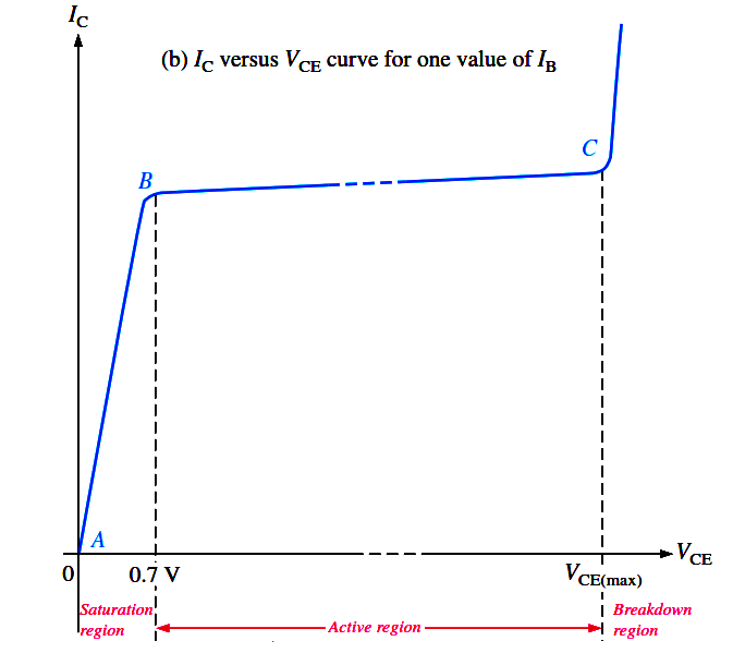
Ideally, when VCE exceeds 0.7 V, the base-collector junction becomes reverse-biased and the transistor goes into the active, or linear, region of its operation. Once the base-collector junction is reverse-biased, IC levels off and remains essentially constant for a given value of IB as VCE continues to increase. Actually, IC increases very slightly as VCE increases due to widening of the base-collector depletion region. This results in fewer holes for recombination in the base region which effectively causes a slight increase in βDC. This is shown by the portion of the characteristic curve between points B and C in Figure (b). For this portion of the characteristic curve, the value of IC is determined only by the relationship expressed as IC = βDCIB.

When VCE reaches a sufficiently high voltage, the reverse-biased base-collector junction goes into breakdown; and the collector current increases rapidly as indicated by the part of the curve to the right of point C in Figure (b). A transistor should never be operated in this breakdown region.

Transistor Characteristic Curves

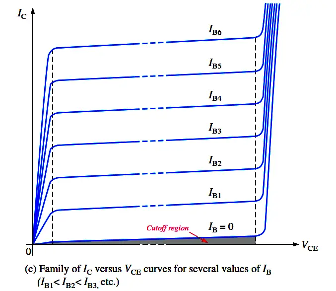
A family of collector characteristic curves is produced when IC versus VCE is plotted for several values of IB, as illustrated in Figure (c). When IB = 0, the transistor is in the cutoff region although there is a very small collector leakage current as indicated. Cutoff is the nonconducting state of a transistor. The amount of collector leakage current for IB = 0 is exaggerated on the graph for illustration.

Don't Miss Our Updates
Be the first to get exclusive content straight to your email.
We promise not to spam you. You can unsubscribe at any time.
Invalid email address
You've successfully subscribed !

Continue Reading

Transistor as an Amplifier in Common Emitter
Diode Limiters/Clippers Operation
Half Wave Voltage Doubler using Diodes
Capacitively Coupled Multistage Transistor Amplifier
Phototransistor Working Principle
Center Tapped Full Wave Rectifier Operation
Share This Article
Facebook Whatsapp Whatsapp LinkedIn Copy Link
Share
Leave a Comment

Leave a Reply Cancel reply

Your email address will not be published. Required fields are marked *

Stay Connected

128.3kFollowersLike
69.1kFollowersFollow
210kSubscribersSubscribe
38kFollowersFollow

Categories

Explore More

Diode Clampers Principle
Full Wave Bridge Rectifier Operation
Cathode Ray Tube Deflection System
Transistor Collector Feedback Bias
Zener Diode Breakdown Characteristics
Operation of Zener Diode Voltage Regulator
Diodes Voltage Quadrupler
Positive & Negative Diode Clippers

Keep Learning

Fluorescent Screen of CRT

CRT Fluorescent Screen

Voltage Divider Rule

Voltage Divider Rule

What is a Memristor

What is a Memristor? Principle, Advantages, Applications

pn-junction-energy-diagrams

Energy Diagrams of PN Junction & Depletion Region

PIN Diode Working Principle

PIN Diode Working Principle

Reverse Bias Diode Working Animation

Forward Bias & Reverse Bias Diode Working Animation

Combining Independent Current Sources in Parallel

Combining Independent Current Sources in Parallel

Comparison of Half wave Rectifiers and Full wave Rectifiers

Comparison of Half wave Rectifiers and Full wave Rectifiers

Learn More

What Every Instrument Engineer Should Know

Common Mistakes in Instrumentation

Fail-Close Valve

What is a Fail-Close Valve? – Advantages and Disadvantages

Measuring Instruments MCQ

Measuring Instruments MCQ

Free Online Control Valves Course

Free Control Valves Course

Electrical Machines Questions and Answers

Electrical Machines Losses, Efficiency and Regulation Questions

Digital Electronics Multiple Choice Questions

Memory Devices Objective Questions – Part 5

Pressure Gauge with Syphons

Pressure Gauge Syphons Principle

Digital Electronics Objective Questions

Number Systems Multiple Choice Questions

Menu

  • About
  • Privacy Policy
  • Copyright

Quick Links

  • Learn PLC
  • Helping Hand
  • Part Time Job

YouTube Subscribe

Follow US
All rights reserved. Reproduction in whole or in part without written permission is prohibited.
Welcome Back!

Sign in to your account

Username or Email Address
Password

Lost your password?