A Functional Block Diagram or FBD is a graphical representation of process flow using simple interconnecting blocks. It is similar to the Ladder Logic diagram except the function block replaces the interconnection of contacts and the coils.
In addition to this, Functional Block Diagram has any rung or rail. A functional Block diagram circuit is an analog to an electrical circuit where links and wires represent signal paths between the components.
These Functional Block diagrams are a graphical representation of executable code. A functional block can take one or more inputs and make decisions and generate two or more outputs.
There are many different types of Functional Blocks included in the programming software to perform various common tasks.
Functional Block Diagram for Logic Gates
Like all digital equipment, PLC also operates on the binary principle. The term binary represents that it has only two states. These states are ‘0’ and ‘1’, in this ‘0’ represents the OFF state or False or Low condition, and ‘1’ represents the ON state or True or High condition.
A Logic Gate is a circuit with several inputs but only one output is activated by particular combinations of input conditions. The two-state binary conditions were applied to the gates for making decisions for providing the output.
Logic Gates
Here we will discuss the following logic gates design in the functional block diagram language of a PLC.
- AND GATE
- OR GATE
- NOT GATE
- NAND GATE
- NOR GATE
- X-OR GATE
- X-NOR GATE
AND Gate
An AND GATE has two or more inputs but it has only one output. The Output assumes the logic ‘1’ state, only when every one of its inputs is at the logic ‘1’ state. The output assumes the logic ‘0’ state even if one of its inputs is at the logic ‘0’ state.
The AND GATE is therefore defined as a device whose output is ‘1’, if and only if all its inputs are ‘1’. Hence this AND GATE is also called an all-or-nothing gate.
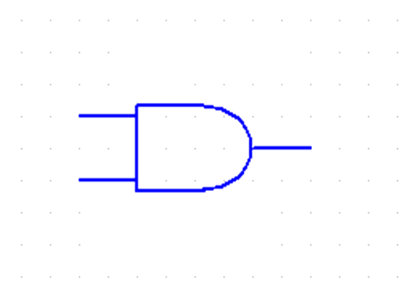
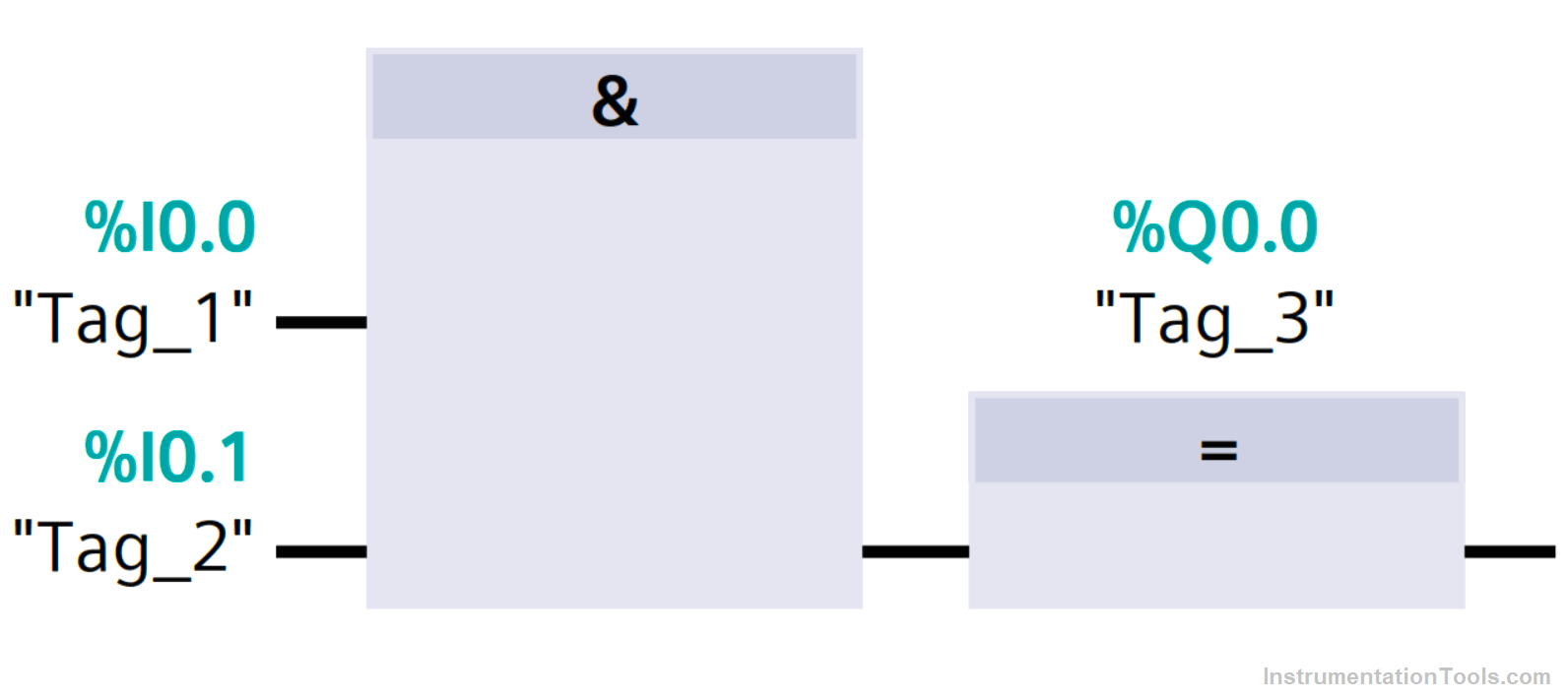
The logic symbol, Truth Table, and Functional Block Diagram of AND GATE are shown below. In this, we want to note that the output is ‘1’ only when all the inputs were ‘1’.
Logic Symbol of AND Gate
Truth Table of AND Gate
| Input 1 (I0.0) | Input 2 (I0.1) | Output (Q0.0) |
| 0 | 0 | 0 |
| 0 | 1 | 0 |
| 1 | 0 | 0 |
| 1 | 1 | 1 |
Functional Block Diagram of AND Gate
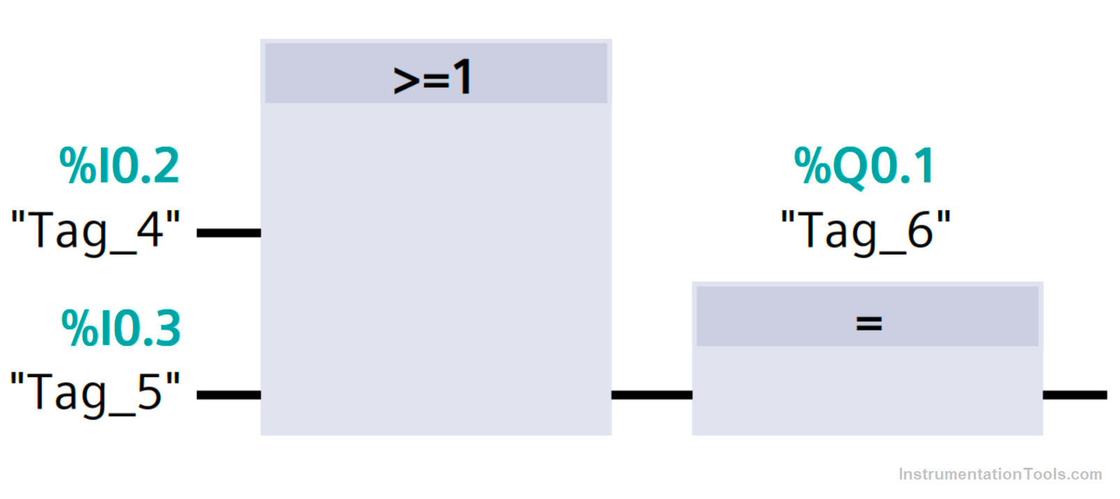
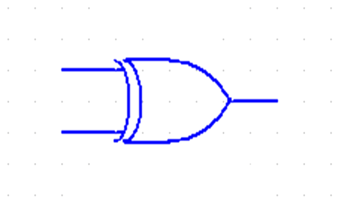
OR Gate
Like an AND GATE, an OR GATE may have two or more inputs but it has only one input. The output assumes the logic ‘1’ state, even if one of its inputs is in the logic ‘1’ state. Its output assumes the logic ‘0’ state, only when each one of its inputs is in the logic ‘0’ state.
An OR GATE may therefore be defined as a device whose output is ‘1’, even if one of its inputs is ‘1’. Hence an OR GATE is also called any or all gate.
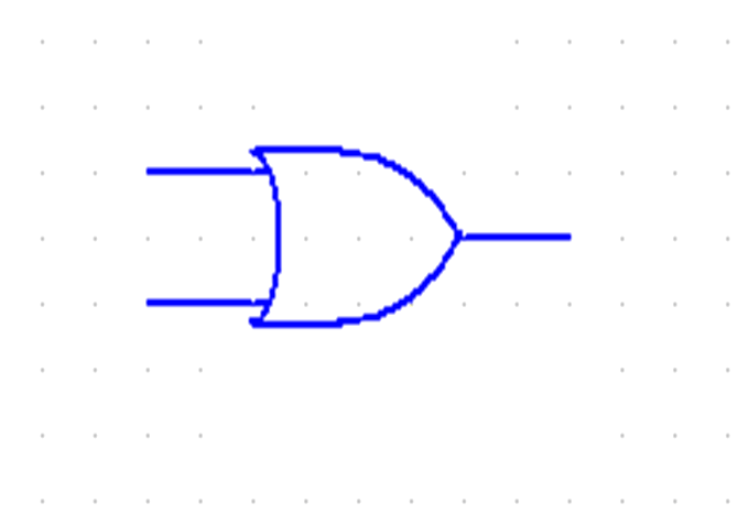
The logic symbol, Truth Table, and Functional Block Diagram of OR GATE are shown below. In this, we want to note that the output is ‘1’ even if one of the inputs was ‘1’.
Logic Symbol of OR Gate
Truth Table of OR Gate
| Input 1 (I0.2) | Input 2 (I0.3) | Output (Q0.1) |
| 0 | 0 | 0 |
| 0 | 1 | 1 |
| 1 | 0 | 1 |
| 1 | 1 | 1 |
Functional Block Diagram of OR Gate
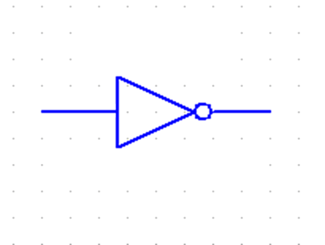
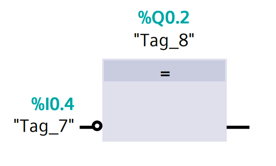
NOT Gate
A NOT GATE also called an inverter, has only one input and of course, it has only one output.
In NOT GATE its output always complements its input. That is, the output of a NOT GATE assumes the logic state ‘1’ when its input is in logic state ‘0’ and assumes the logic state ‘0’ when its input is in logic state ‘1’.
The logic symbol, Truth Table, and Functional Block Diagram are shown below figures respectively.
Logic Symbol of NOT Gate
Truth Table of NOT Gate
| Input (I0.4) | Output (Q0.2) |
| 0 | 1 |
| 1 | 0 |
Functional Block Diagram of NOT Gate
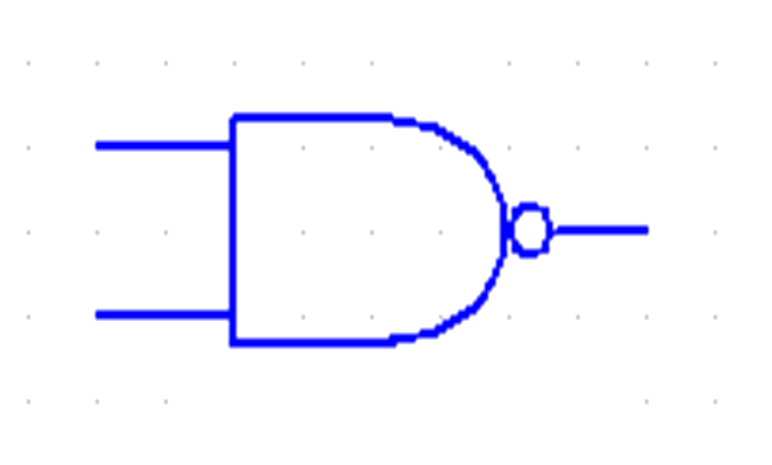
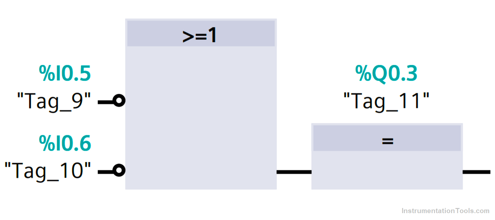
NAND Gate
NAND means a combination of NOT GATE & AND GATE, this means the output of the AND GATE is inverted.
So, NAND GATE is a mix of NOT GATE & AND GATE. In fact, NAND is the contraction of the word NOT-AND. In this NAND, the output is a logic ‘0’ level only when each of the inputs assumes a logic ‘1’ level.
For any other combinations of inputs, the output is a logic ‘1’ level. Below given diagrams represents the Logical Symbol, Truth Table, and Functional Block diagram of NAND GATE.
Logic Symbol of NAND Gate
Truth Table of NAND Gate
| Input 1 (I0.5) | Input 2 (I0.6) | Output (Q0.3) |
| 0 | 0 | 1 |
| 0 | 1 | 1 |
| 1 | 0 | 1 |
| 1 | 1 | 0 |
Functional Block Diagram of NAND Gate
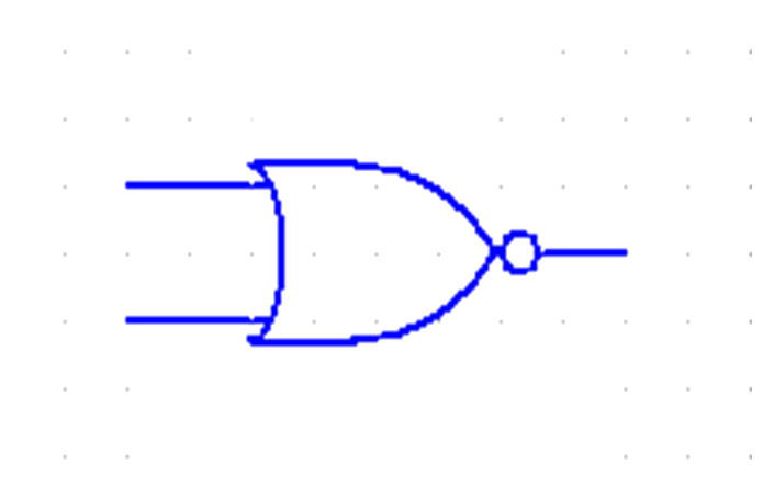
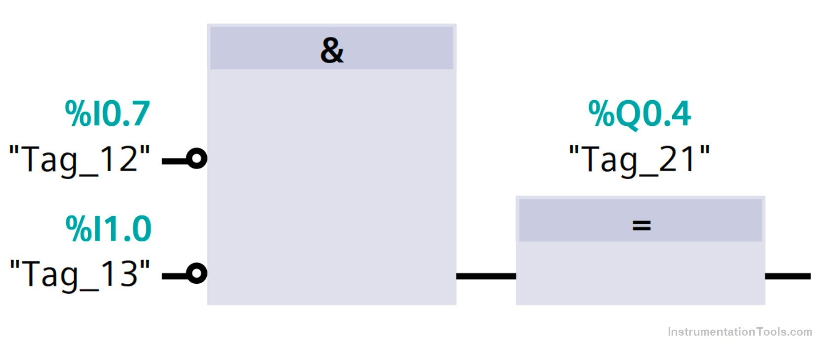
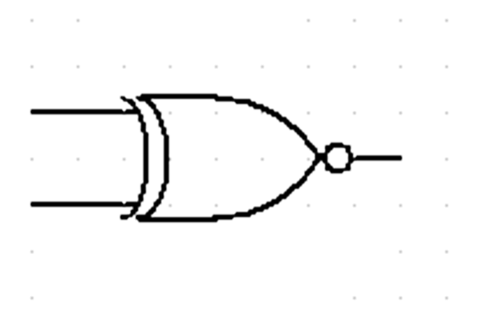
NOR Gate
NOR GATE means a mix of NOT & OR, that is the output of the OR GATE is inverted. So, a NOR GATE is a combination of NOT and OR GATE.
The NOR is simply a contraction of the word NOT-OR. The output of NOR GATE is at logic ‘1’ level only when all the inputs are at logic ’0’ level and in other combinations, the output of NOR GATE is always at logic ‘0’ level only.
This NOR gate has two or more inputs but it has only one output.
Logic Symbol of NOR Gate
Truth Table of NOR Gate
| Input 1 (I0.7) | Input 2 (I1.0) | Output (Q0.4) |
| 0 | 0 | 1 |
| 0 | 1 | 0 |
| 1 | 0 | 0 |
| 1 | 1 | 0 |
Functional Block Diagram of NOR Gate
XOR Gate
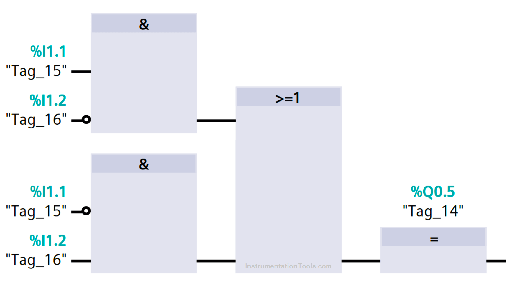
An X-OR GATE is a two-input and one-output logic circuit, whose output assumes a logic ‘1’ state when one and only one of its two inputs assumes a logic’1’ state.
Under the conditions when both the inputs assume the logic ‘0’ state or when both the inputs assume the logic ‘1’ state then the output assumes a logic ‘0’ state.
As X-OR GATE produces an output ‘1’ only when the inputs are not equal, it is called an anti-coincidence gate or inequality detector. The output of an X-OR GATE is a modulo sum of its two inputs.
The name Exclusive-OR (X-OR) is derived from the fact that its output is a ‘1’ only when exclusively one of its inputs is a ‘1’. In this X-OR GATE, three or more input variables do not exist.
Logic Symbol of XOR Gate
Truth Table of XOR Gate
| Input 1 I 1.1 | Input 2 I 1.2 | Output Q0.5 |
| 0 | 0 | 0 |
| 0 | 1 | 1 |
| 1 | 0 | 1 |
| 1 | 1 | 0 |
Functional Block Diagram of XOR Gate
XNOR Logic Gate
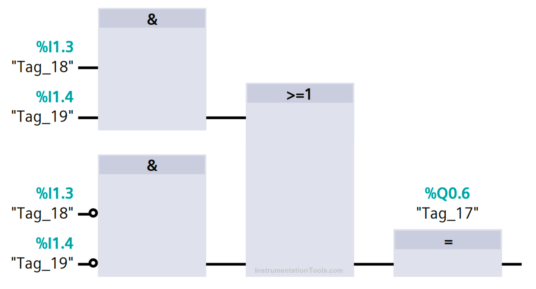
An X-NOR GATE is a combination of X-NOR GATE and NOT GATE. The X-NOR gate is a two-input and one-input logic circuit. In this output assumes a ‘1’ state only when both the inputs assume a ‘0’ state or when both the inputs assume a ‘1’ state.
The output assumes a ‘0’ state when one of the inputs assumes a ‘0’ state and the other input assume a ‘1’ input. It is also called a coincidence gate because its output is 1 only when its input coincides.
EXNOR can be used as an equality detector because its output is ‘1’ only when its inputs are equal. Three or more variables in X-NOR do not exist, it will function for two inputs only.
Logic Symbol of XNOR Logic Gate
Truth Table of XNOR Logic Gate
| Input 1 (I1.3) | Input 2 (I1.4) | Output (Q0.6) |
| 0 | 0 | 1 |
| 0 | 1 | 0 |
| 1 | 0 | 0 |
| 1 | 1 | 1 |
Functional Block Diagram of XNOR Logic Gate
If you liked this article, then please subscribe to our YouTube Channel for Instrumentation, Electrical, PLC, and SCADA video tutorials.
You can also follow us on Facebook and Twitter to receive daily updates.
Read Next:
- Automation Documents
- Delta PLC & VFD Modbus
- Compare PLC and SCADA
- PLC and DCS System Checks
- DCS System Maintenance