Inst ToolsInst ToolsInst Tools
  • Courses
  • Automation
    • PLC
    • Control System
    • Safety System
    • Communication
    • Fire & Gas System
  • Instrumentation
    • Design
    • Pressure
    • Temperature
    • Flow
    • Level
    • Vibration
    • Analyzer
    • Control Valve
    • Switch
    • Calibration
    • Erection & Commissioning
  • Interview
    • Instrumentation
    • Electrical
    • Electronics
    • Practical
  • Q&A
    • Instrumentation
    • Control System
    • Electrical
    • Electronics
    • Analog Electronics
    • Digital Electronics
    • Power Electronics
    • Microprocessor
  • Request
Search
  • Books
  • Software
  • Projects
  • Process
  • Tools
  • Basics
  • Formula
  • Power Plant
  • Root Cause Analysis
  • Electrical Basics
  • Animation
  • Standards
  • 4-20 mA Course
  • Siemens PLC Course
Reading: SCR Switching Characteristics
Share
Font ResizerAa
Inst ToolsInst Tools
Font ResizerAa
  • Courses
  • Design
  • PLC
  • Interview
  • Control System
Search
  • Courses
  • Automation
    • PLC
    • Control System
    • Safety System
    • Communication
    • Fire & Gas System
  • Instrumentation
    • Design
    • Pressure
    • Temperature
    • Flow
    • Level
    • Vibration
    • Analyzer
    • Control Valve
    • Switch
    • Calibration
    • Erection & Commissioning
  • Interview
    • Instrumentation
    • Electrical
    • Electronics
    • Practical
  • Q&A
    • Instrumentation
    • Control System
    • Electrical
    • Electronics
    • Analog Electronics
    • Digital Electronics
    • Power Electronics
    • Microprocessor
  • Request
Follow US
All rights reserved. Reproduction in whole or in part without written permission is prohibited.
Inst Tools > Blog > Power Electronics > SCR Switching Characteristics

SCR Switching Characteristics

Last updated: September 19, 2016 4:23 am
Editorial Staff
Power Electronics
No Comments
Share
6 Min Read
SHARE

SCR Switching Characteristics or Dynamic Characteristics:

  • The switching characteristics are important particularly at high-frequency, to define the device velocity in changing from conduction state to blocking state and vice versa.
  • Losses occurring in the device during switching from ON state to OFF state and OFF state to ON state is known as Switching Losses.
  • The device’s switching characteristics tells us about the switching losses, which is very important parameter to decide the selection of device.
  • At high frequency, the switching losses are more.
  • This post will discuss about thyristor switching characteristics in detail. It is recommended to read Thyristor-Basics & V-I Characteristics for proper understanding of thyristor switching characteristics.

Turn ON mechanism:-

  • When a positive gate signal is applied to a forward biased SCR, the transition of SCR from blocking state to conducting state is called as turn ON mechanism.
  • The time taken for SCR to traverse from the blocking state to conducting state is called as turn on time.
  • Turn on time is divided into 3 periods.
  • tON = td + tr + tp
  • td = delay time, tp or ts = peak time (or) spread time
  • when the gate current reaches 0.9IG the anode current IA starts increasing and reaches 0.1IA (10% of its max value)
  • The time taken for anode current to reach 0.1IA is called as delay time(td).
  • In other words, it is the time taken for anode voltage to fall from VA to 0.9VA
  • The anode current further increases and reaches 0.9IA.
  • The time taken by the anode current to increases from 0.1IA to 0.9IA is called as rise time(tr).
  • In other words, it is the time taken by the anode voltage to fall from 0.9VA to 0.1VA

Spread Time or Peak time (ts or tp)

  • It is time taken by the anode current to rise from ( 0.9IA to maximum value of IA) 90% to 100% of its full value. (or)
  • It is the time taken by VA to fall from 0.1VA to it’s ON state voltage drop(near by zero).
  • During this time the conduction spreads over the entire cross-section of cathode and so electrons spread over all the junctions.
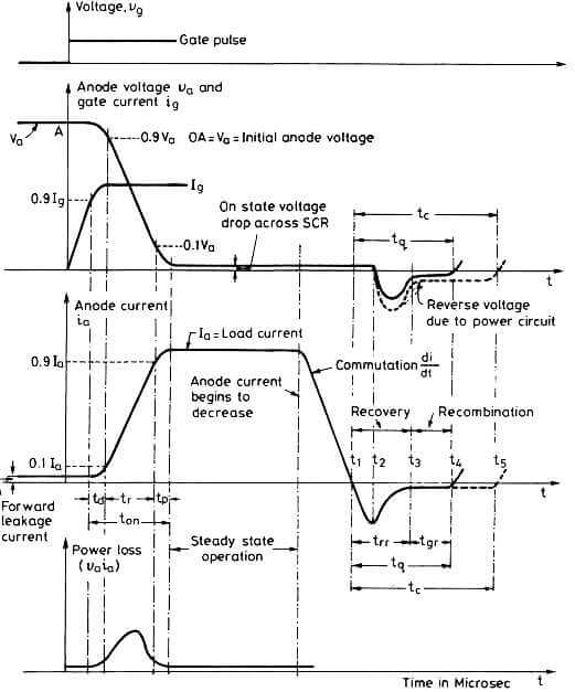
SCR Switching Characteristics

Turn OFF mechanism:

  • Turning OFF an SCR means bringing the SCR from conducting state to blocking state.
  • To turn off an SCR two things are to be done
    (1) Reduce the anode current below its holding current level.
    (2) Application of reverse voltage.
  • When the anode current is zero, if we apply forward voltage to the SCR, the device will not be able to block this forward voltage due to the fact that excess charge carriers are still at the junctions, so the device will start conducting even when the gate signal is not applied.
  • In order to avoid this, reverse biasing of SCR is done to remove the excess charge carriers from all four layers.
  • The turn OFF time is defined as the time from the instant the anode current becomes zero to the instant SCR reaches its forward blocking ability.
    Turn off time tOFF = trr + tgr
    trr = Reverse recovery time
    tgr =Gate recovery time
    Reverse recovery process is the removal of excessive charge carries from the top and bottom layers of SCR.

          At t1; current IA = 0

  • After t1; IA build up in the reverse direction, due to the charge carriers stored in the four layers.
  • Reverse recovery current removes the excessive carriers from junctions J1 and J3 during the time t1 to t3. (Reverse recovery current flows due sweeping out of holes from top p-layer and electrons from bottom n layer)

Reverse Recovery Time (trr):-

  • It is the time taken for the removal of excessive carriers from top and bottom layer of SCR.
  • At t2: When nearly 60% of charges are removed from the outer two layers, the reverse recovery current decreases.
  • This decaying causes a reverse voltage to be applied across the SCR.
  • At t3 all excessive carriers from J1 and J3 is removed.
  • The reverse voltage across SCR removes the excessive carriers from junction J2.
  • Gate recovery process is the removal of excessive carriers from J2 junction by application of reverse voltage.
  • Time taken for removal of trapped charges from J2 is called gate recovery time(tgr).
  • At t4 all the carriers are removed and the device moves to the forward blocking mode.
Don't Miss Our Updates
Be the first to get exclusive content straight to your email.
We promise not to spam you. You can unsubscribe at any time.
Invalid email address
You've successfully subscribed !

Continue Reading

Phase-Controlled Half-Wave Rectifier With Freewheeling Diode
Power Electronics Objective Questions
Power MOSFET – Symbol, Types, Working, Characteristics, Advantages
R R-C Firing Circuits Disadvantages
Thyristor Commutation Techniques – Types, Working Principles
What is Power Electronics? Evolution, Block Diagram, Advantages
Share This Article
Facebook Whatsapp Whatsapp LinkedIn Copy Link
Share
Leave a Comment

Leave a Reply Cancel reply

Your email address will not be published. Required fields are marked *

Stay Connected

128.3kFollowersLike
69.1kFollowersFollow
210kSubscribersSubscribe
38kFollowersFollow

Categories

Explore More

Thyristor Interview Questions & Answers
Power Diode – Characteristics, Construction, Working, Advantages
Power Electronics – Phase Controlled Half Wave Rectifier RL Load
Turning Off SCR – Commutation
MCT (MOS Controlled Thyristor) – Symbol, Working, Characteristics, Advantages
Power Electronic Devices Specification and Classification
Thyristor Protection Circuits (SCR) – Types, Principle, Explanation
Basics of Thyristor

Keep Learning

Half-controlled Rectifier With R Load

Phase Controlled Rectifier – Half Controlled Rectifier with R Load

RC snubber circuits

How Snubber Circuit works ?

Symbol of Transistor

Power Transistor – Structure, Biasing, Characteristics, Advantages

Static VI Characteristics of Thyristor

Thyristors – Working, VI Characteristics, Turn ON Methods

Procedure to test the TRIAC

How to Test TRIAC with Multimeter

RC Triggering

SCR Triggering Methods

Full-Controlled Rectifier Working Principle

Single-Phase Mid-Point Converter – Bridge Rectifier with Center Tap

Two Transistor Model of Thyristor

Thyristors – Switching, Two Transistor Model, Advantage, Applications

Learn More

Frequency Response MCQ

Bode Plots MCQ

MOS Gas Sensor Principle

MOS Type Gas Sensor Principle

Transistor Amplifier Working Principle

Web SCADA HMI

Web-based SCADA HMI Software

pH Analyzers Interview Questions Answers

pH Analyzer Interview Questions and Answers

Fired Boiler Induced Draft Fan (IDF) Failures

Fired Boiler Induced Draft Fan (IDF) Failures Upset all Plants Operations

Blowdown Valve (BDV) and Shutdown Valve (SDV)

Difference between Blowdown Valve (BDV) and Shutdown Valve (SDV) ?

Identify Problem with Oily Water Filter Instrumentation

Identify Problem with Oily Water Filter Instrumentation

Menu

  • About
  • Privacy Policy
  • Copyright

Quick Links

  • Learn PLC
  • Helping Hand
  • Part Time Job

YouTube Subscribe

Follow US
All rights reserved. Reproduction in whole or in part without written permission is prohibited.
Welcome Back!

Sign in to your account

Username or Email Address
Password

Lost your password?