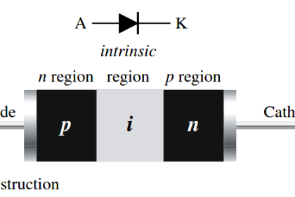
When you take a block of silicon and dope part of it with a trivalent impurity and the other part with a pentavalent impurity, a boundary called the pn junction is formed between the resulting p-type and n-type portions. The pn junction is the basis for diodes, certain transistors, solar cells, and other devices.
A p-type material consists of silicon atoms and trivalent impurity atoms such as boron. The boron atom adds a hole when it bonds with the silicon atoms. However, since the number of protons and the number of electrons are equal throughout the material, there is no net charge in the material and so it is neutral.
An n-type silicon material consists of silicon atoms and pentavalent impurity atoms such as antimony. As you have seen, an impurity atom releases an electron when it bonds with four silicon atoms. Since there is still an equal number of protons and electrons (including the free electrons) throughout the material, there is no net charge in the material and so it is neutral.
If a piece of intrinsic silicon is doped so that part is n-type and the other part is p-type, a pn junction forms at the boundary between the two regions and a diode is created, as indicated in Figure (a). The p region has many holes (majority carriers) from the impurity atoms and only a few thermally generated free electrons (minority carriers). The n region has many free electrons (majority carriers) from the impurity atoms and only a few thermally generated holes (minority carriers).
Fig : Formation of the depletion region. The width of the depletion region is exaggerated for illustration purposes.
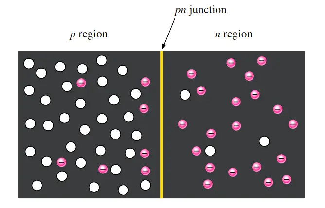
Fig: (a) The basic silicon structure at the instant of junction formation showing only the majority and minority carriers. Free electrons in the n region near the pn junction begin to diffuse across the junction and fall into holes near the junction in the p region.
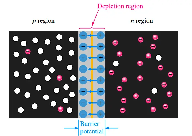
Fig : (b) For every electron that diffuses across the junction and combines with a hole, a positive charge is left in the n region and a negative charge is created in the p region, forming a barrier potential. This action continues until the voltage of the barrier repels further diffusion. The blue arrows between the positive and negative charges in the depletion region represent the electric field.
Formation of the Depletion Region
The free electrons in the n region are randomly drifting in all directions. At the instant of the pn junction formation, the free electrons near the junction in the n region begin to diffuse across the junction into the p region where they combine with holes near the junction, as shown in Figure (b).
Before the pn junction is formed, recall that there are as many electrons as protons in the n-type material, making the material neutral in terms of net charge. The same is true for the p-type material.
When the pn junction is formed, the n region loses free electrons as they diffuse across the junction. This creates a layer of positive charges (pentavalent ions) near the junction. As the electrons move across the junction, the p region loses holes as the electrons and holes combine. This creates a layer of negative charges (trivalent ions) near the junction. These two layers of positive and negative charges form the depletion region, as shown in Figure (b). The term depletion refers to the fact that the region near the pn junction is depleted of charge carriers (electrons and holes) due to diffusion across the junction. Keep in mind that the depletion region is formed very quickly and is very thin compared to the n region and p region.
After the initial surge of free electrons across the pn junction, the depletion region has expanded to a point where equilibrium is established and there is no further diffusion of electrons across the junction. This occurs as follows. As electrons continue to diffuse across the junction, more and more positive and negative charges are created near the junction as the depletion region is formed. A point is reached where the total negative charge in the depletion region repels any further diffusion of electrons (negatively charged particles) into the p region (like charges repel) and the diffusion stops. In other words, the depletion region acts as a barrier to the further movement of electrons across the junction.
Barrier Potential
Any time there is a positive charge and a negative charge near each other, there is a force acting on the charges as described by Coulomb’s law. In the depletion region there are many positive charges and many negative charges on opposite sides of the pn junction. The forces between the opposite charges form an electric field, as illustrated in Figure (b) by the blue arrows between the positive charges and the negative charges. This electric field is a barrier to the free electrons in the n region, and energy must be expended to move an electron through the electric field. That is, external energy must be applied to get the electrons to move across the barrier of the electric field in the depletion region.
The potential difference of the electric field across the depletion region is the amount of voltage required to move electrons through the electric field. This potential difference is called the barrier potential and is expressed in volts. Stated another way, a certain amount of voltage equal to the barrier potential and with the proper polarity must be applied across a pn junction before electrons will begin to flow across the junction.
The barrier potential of a pn junction depends on several factors, including the type of semiconductive material, the amount of doping, and the temperature etc.