What is a PN junction diode?
The name PN junction diode stands for a junction termed as PN junction formed by injecting into one side of intrinsic semiconductor crystal acceptor impurities (forming a p-type semiconductor )and donor impurities from the other side(forming an n-type semiconductor) with two active terminals (di means two) of one terminal acts as anode (p-type) and other as cathode (n-type).
What is a Junction capacitance of a diode?
The increase or decrease of uncovered charge at the junction in depletion layer region can be considered a capacitive effect and is termed as junction capacitance. On the either side of depletion region the combination of charged ions (acceptor atoms in p-region by accepting diffused electrons from n-region becomes positively charged and the donor atoms by accepting the diffused holes from p-type region becomes positively charged) acts as a parallel plate capacitor. Any variation in the applied voltage causes a corresponding change in charge stored in the depletion region, Hence the junction capacitance is given as Cj = dqj / dvj where dqj is variation in charge stored in depletion region due to variation in voltage applied across junction dvj.
What is diffusion capacitance or Transit time capacitance?
The rate of change of injected charge stored near the junction outside depletion region with applied voltage is called diffusion or Transit time or storage capacitance.
Cd = dQ/dV
dQ is the change in the injected minority charge store near the junction outside depletion region. Assume for simplicity p material is heavily doped compared to n material. In such a case the injected electron current in to p side is negligible compared to injected hole current to n side across the junction. Therefore the hole current in terms of total injected charge is given by
I = Q/t where t is life time of holes
Hence the diffusion capacitance of diode is given by
Cd = dQ/dV = t*(dI/dV) = t/rd
Cd = t*I / (η*Vt)
What is a diode static and dynamic resistance?
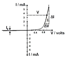
Static resistance of a diode is the ratio of voltage across the diode to the current through the diode. It varies with bias point on the V-I characteristic curve of diode.
Static resistance rs = V/I
Dynamic resistance of a diode at a particular bias point (V, I) is defined as inverse of slope of V-I characteristics of diode corresponding to that voltage across the diode and current through the diode.
Dynamic resistance rd = dV/dI
Static resistance of the diode varies with the bias point whereas Dynamic resistance of a diode is constant over a wide range of bias points.
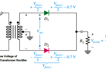
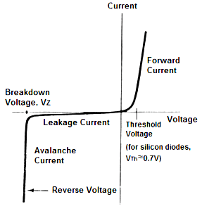
What is Reverse Break down (VBD) voltage of a diode?
The Reverse Break down (VBD) voltage of a diode is defined as the reverse bias voltage across the diode at which it starts conducting currents heavily. At voltages greater than Reverse Break down voltage the diode currents increase for even a small change in reverse bias voltage. Sufficient heat sink has to be provided to remove the heat dissipated at the diode junction for voltages greater than Reverse Break down voltage; otherwise it will lead to permanent damage of diode
What are Reverse break down mechanisms in a diode?
There are two Reverse break down mechanisms in a diode. They are
- Avalanche Breakdown
- Zener breakdown
What are high frequency diodes?
Diodes which support high frequency switching are called as high frequency diodes. The following diodes are some of high frequency diodes:
- PIN diode
- Schottky diode
- Tunnel diode.
Why direct band gap semiconductors are used in LED?.
In direct band gap semiconductors most of the energy released after an electron in conduction band recombines with a hole in valence band will be in the form of light energy whereas In indirect band gap semiconductors most of the energy released after an electron in conduction band recombines with a hole in valence band will be in the form of heat energy Hence direct band gap semiconductors are used in Light emitting diodes. Some of the direct band gap semiconductors used in the manufacture of LED’s are direct band gap semiconductors gallium antimonide (GaSb), gallium arsenide (GaAs), indium phosphide (InP) e.t.c
What is drift current?
The Flow of charge carriers under the influence of applied electric field is called as drift current. Magnitude of Drift current depends on the mobility, concentration, magnitude of applied electric field and the cross sectional area through which the current is flowing. The equation for drift current density for electrons and holes is given by
Jn = q*μn*n*E,
for holes Jp = q*μp*p*E
Where μn, μp are mobilities of electrons and holes, n, p are electron and hole concentrations, E is applied electric field.
What s diffusion current?
The flow of charge carriers owing to the presence of concentration gradient due to diffusion is termed as diffusion current. This diffusion current flows from high concentration side to low concentration side. Diffusion current is purely a statistical phenomenon. Diffusion current density is directly proportional to concentration gradient (concentration gradient is the rate at which the concentration of carriers varies with distance dp/dx or dn/dx) and is given by
Jn= Dn*q* dn/dx for electrons
Jp= -Dp*q* dp/dx for holes
Where Dn, Dp are diffusion constants for holes and electrons, q is electron charge, dp/dx, dn/dx is concentration gradient for holes and electrons.
What is storage time, forward and reverse recovery times of diode?
The forward recovery time of a diode is defined as the time difference between the 10 % point of diode final voltage and the time when the diode voltage reaches 90 % and remains within 10 % of final value.
The terms storage and transition times are used when diode is suddenly switched from forward bias to reverse bias.
Storage time is defined as the time interval between application of reverse bias and the time at which stored minority charge becomes zero.
Transition time is defined as the time the diode transition capacitance takes to charge from zero (This happens when stored minority charge becomes zero) to applied reverse bias.
The total time elapsed between the application of reverse bias till the diode charge fully to applied reverse bias is called as reverse recovery time. It is the sum of storage time and transition time.
What is current equation of diode?
The current equation of a diode is given by
Id = Ido*(exp (V/Vt)-1)
where
Ido is reverse saturation current,
V is voltage applied across diode,
Vt is the voltage equivalent of temperature.
If V is negative and V >> Vt exp (V/Vt) tends to zero and Ic = -Ico.
What is reverse saturation current in diode?
It is the current flowing through the diode when diode is reverse biased with a voltage greater than 5*Vt (0.13 volts at room temperature) where Vt is the voltage equivalent of temperature which is 26 milli volts at room temperature. Reverse saturation current is minority carrier current resulting from flow of minority carriers from either side of junction (electrons from p-side to n-side and holes from n-side to p-side). It is a function minority carrier concentrations on either side i.e. electrons in p-type semiconductor and holes in n-type semiconductor, carrier life times and diffusion constants.
How reverse current varies with temperature?
The reverse saturation current of a diode is a sensitive function of temperature and increases rapidly with increasing temperatures. It is because the reverse saturation current increases with increasing conductivity of silicon material using in manufacturing the transistor. The conductivity in turn depends on free electron and hole concentrations which increases as temperature increases due to increased thermal energies of electrons(due to increased temperatures). Approximately the reverse saturation current doubles for every 10 Deg C rise in temperature. If Ico1 is the reverse saturation current at temperature T1, then at temperature T2 the reverse saturation current is given by
Ico2= Ico1*2(T2-T1)/10
What is continuity equation?
The continuity equation governs the functional relationship of carrier concentrations for applied voltage (or) current inputs in the semiconductor body with time and distance. It is based on law of conservation of charge. The continuity equation for holes is given as
p/ t = ((p0-p)/tp) – (1/q)* Jp/ x
Where p is hole concentration which is function of distnce and time, p0 = g* tp,g is holes generated per volume due to thermal generation, Jp is hole current.The continuity eqaution is simlar for elctrons with p replaced by n.
What is built in potential of diode?
ANS: The potential developed across a open circuited PN junction diode id termed as Built in potential (or) contact potential. For a PN junction diode this is given as
V0 = Vt*ln (Na*Nd/ni^2)
What is law of junction?
The law of junction states that in a semiconductor bar with two points at potentials V1 and V2 with concentrations P1 and P2, then P1 and P2 are related to V1 and V2 by
P1 = P2*exp ((V2-V1)/Vt), Where Vt is voltage equivalent of temperature
Explain the signification of η in diode current equation?
In deriving the current equation for diode the carrier generation and recombination in the space charge region is assumed to be negligible. Such an assumption is valid for germanium but not for silicon. Hence in order to take them into account the factor η factor is introduce in current equation.
What is the η value for germanium and silicon?
The carrier generation and recombination in the space charge region can be neglected for germanium but not for silicon. Hence
η = 1 for germanium
η = 2 for silicon
Draw the VI characteristics of the diode?
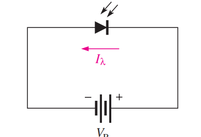
Which diodes will operate in reverse bias?
Following are the some of the diodes which operate in reverse bias
a) Zener diode
b) PIN Diode
c) Varactor diode
What is Diffusion length of electrons and holes?
The average distance hole or electron travels before it recombines with electron or hole subsequently is called as diffusion length of holes or electrons. This is denoted as Lp (holes) and Ln (electrons). The unit is Meters.
Define Carrier Life time of holes (or) elections in a semiconductor?
The average time a minority carrier hole (or) electron survives before it recombines is called carrier life time.
What is the Relation between diffusion constant lifetime and diffusion length in diode?
Diffusion length Lp=Root (Dp * Tp)
Where Lp = Diffusion length of holes in meters
Dp = Diffusion constant of holes in m2/s
Tp = Carrier life time of hole sec
What is Einstein’s relationship between diffusion constant and mobility?
The Einstein’s relationship between diffusion constant and mobility is
Where Dp, Dn are diffusion constants for holes and electrons; µn, µp are mobilities of electrons and holes, Vt is voltage equitant of temperature.
What is voltage equivalent of temperature and its value at room temperature?
The voltage equivalent of temperature is defined as
Vt = K*T/q
Where K is Boltzmann constant = 1.38*10^-23 joule/Kelvin
T is absolute temperature in Kelvin
Q is electronic charge = 1.6*10^-19 coulombs
At room temperature of 27 Deg C (300 K) it is approximately equal to 26 milli volts.
What is low level minority carrier injection in diode?
The term low level minority carrier injection is used when the injected minority carrier concentration (holes in n material, electrons in p material) is very less compared to majority carrier concentration i.e. doping level. For example holes are injected into n type semiconductor due to some excitation say electric filed low level injection condition is satisfied when injected hole concentration << electron concentration.
Which diffusion current dominates the total current under low level minority carrier injection?
Under the assumption of low level injection diffusion current dominates over the drift current.
What is the Electric field across the open circuited diode?
In an open circuited diode the total current flowing through the junction will be zero. Hence there should exist a electric filed to drive drift current to counter act diffusion current as the net current flowing through the junction should be zero. Equating the hole current density to zero
Jp= -Dp*q* dp/dx+ q*μp*p*E
Rearranging the terms we get Eoc = (Dp/ P*μp)* dp/dx, from Einstein’s relationship Hence Eoc = ( / P)* dp/dx.
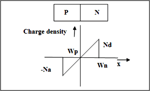
What is abrupt junction or step graded junction?
A PN junction in which the doping changes abruptly from acceptor to donor is defined as abrupt junction. The variation charge density in abrupt junction with Na = Nd is shown below
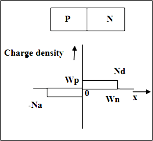
Variation charge density with distance in abrupt junction
What is linear junction?
A PN junction in which the doping changes abruptly from acceptor to donor is defined as abrupt junction. The variation charge density in abrupt junction with Na = Nd is shown below
Variation charge density with distance in linear junction
What is the relation between capacitance and reverse bias voltage?
The capacitance of the reverse bias diode decreases with increase in reverse bias voltage. When a reverse bias voltage increases then the depletion layer width increases which intern decreases the capacitance.
C= ε*A/W
Where W= width of depletion layer.
ε = permittivity of depletion region
A = area of cross section
In general capacitance depends on reverse bias voltage as
C=K (1/ (-V+Vj)^m)
where k is a constant and Vj is built-in potential, V is reverse bias voltage
Where m =1/2 for abrupt junction
m= 1/3for linear junction.
What is the effect of doing on penetration of depletion region?
The depletion rejoin in a PN junction diode penetrates more in to the lightly doped semiconductor (P or N). This can be understood based on charge neutrality principle as follows
Consider a semiconductor junction with P type material having doping concentration Na and N type material with doping concentration of Nd. Let Wp and Wn are the depletion layer widths in P type and N type materials. Then based on law of conservation of charge, The total uncovered charge in a depletion rejoin should be zero. Accordingly
-Na*Wp*Ap +Nd*Wn*An = 0;
Assuming the area of cross sections is equal on either side
Na * Wp = Nd*Wn
From the above equation if Na>> Nd then Wp << Wn hence the depletion penetrates more in to lightly doped N type material.
What are piece wise linear characteristics?
The non liner characteristics of diode can be approximated to piece wise linear characteristics i.e. the relation between voltage and current is defined by two expressions where each expression holds linear for unique interval of range of voltages. The piece wise characteristics of diode are shown below.
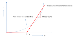
piece wise characteristics of diode
I= 0 for V< 0.7
I= V/Rd for V> 0.7
What are ideal characteristics of a diode?
The following are the ideal characteristics of a diode:
a) The cut-in voltage should be zero.
b) Diode dynamic resistance should be zero
c) Diode capacitance’s should be zero
d) Break down voltage should be infinite e.t.c