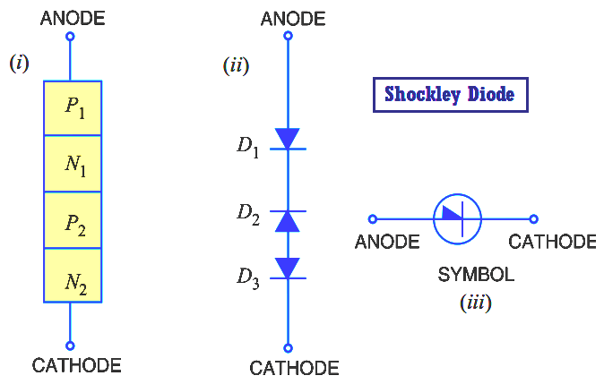
Named after its inventor, a Shockley diode is a PNPN device having two terminals as shown in Fig. (i). This device acts as a switch and consists of four alternate P-type and N-type layers in a single crystal. The various layers are labelled as P1, N1, P2 and N2 for identification. Since a P-region adjacent to an N-region may be considered a junction diode, the Shockley diode is equivalent to three junction diodes connected in series as shown in Fig. (ii). The symbol of Shockley diode is shown in Fig. (iii)
Working
(i) When Shockley diode is forward biased (i.e., anode is positive w.r.t. cathode), diodes D1 and D3 would be forward-biased while diode D2 would be reverse-biased. Since diode D2 offers very high resistance (being reverse biased) and the three diodes are in series, the Shockley diode presents a very high resistance. As the *forward voltage increases, the reverse bias across D2 is also increased. At some forward voltage (called breakover voltage VBO), reverse breakdown of D2 occurs. Since this breakdown results in reduced resistance, the Shockley diode presents a very low resistance. From now onwards, the Shockley diode behaves as a conventional forward-biased diode; the forward cur- rent being determined by the applied voltage and external load resistance. This behaviour of Shockley diode is indicated on its V-I characteristic in Below Fig.
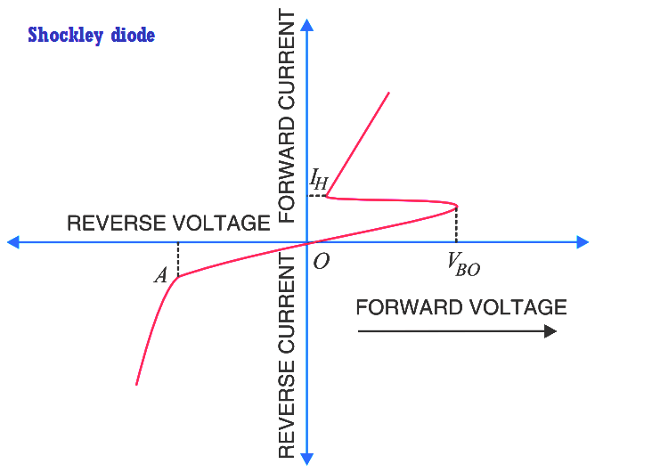
(ii) When Shockley diode is reverse biased (i.e., anode is negative w.r.t. cathode), diodes D1 and D3 would be reverse-biased while diode D2 would be forward-biased. If reverse voltage is increased sufficiently, the reverse voltage breakdown (point A in Above Fig.) of Shockley diode is reached. At this point, diodes D1 and D3 would go into reverse-voltage breakdown, the reverse current flowing through them would rise rapidly and the heat produced by this current flow could ruin the entire device. For this reason, Shockley diode should never be operated with a reverse voltage sufficient to reach the reverse-voltage breakdown point.
Conclusion. The above discussion reveals that Shockley diode behaves like a switch. So long as the forward voltage is less than breakover voltage, Shockley diode offers very high resistance (i.e., switch is open) and practically conducts no current. At voltages above the break-over value, Shockley diode presents a very low resistance (i.e. switch is closed) and Shockley diode conducts heavily. It may be noted that Shockley diode is also known as PNPN diode or four layer diode or reverse- blocking diode thyristor.
Note. Once Shockley diode is turned ON (i.e., it starts conducting), the only way to turn it OFF is to reduce the applied voltage to such a value so that current flowing through Shockley diode drops below its holding current (IH) value. Diode D2 then comes out of its reverse-breakdown state and its high-resistance value is restored. This, in turn, causes the entire Shockley diode to revert to its high- resistance (switch open) state.