Inst ToolsInst ToolsInst Tools
  • Courses
  • Automation
    • PLC
    • Control System
    • Safety System
    • Communication
    • Fire & Gas System
  • Instrumentation
    • Design
    • Pressure
    • Temperature
    • Flow
    • Level
    • Vibration
    • Analyzer
    • Control Valve
    • Switch
    • Calibration
    • Erection & Commissioning
  • Interview
    • Instrumentation
    • Electrical
    • Electronics
    • Practical
  • Q&A
    • Instrumentation
    • Control System
    • Electrical
    • Electronics
    • Analog Electronics
    • Digital Electronics
    • Power Electronics
    • Microprocessor
  • Request
Search
  • Books
  • Software
  • Projects
  • Process
  • Tools
  • Basics
  • Formula
  • Power Plant
  • Root Cause Analysis
  • Electrical Basics
  • Animation
  • Standards
  • 4-20 mA Course
  • Siemens PLC Course
Reading: Power MOSFET Safe Operating Area
Share
Font ResizerAa
Inst ToolsInst Tools
Font ResizerAa
  • Courses
  • Design
  • PLC
  • Interview
  • Control System
Search
  • Courses
  • Automation
    • PLC
    • Control System
    • Safety System
    • Communication
    • Fire & Gas System
  • Instrumentation
    • Design
    • Pressure
    • Temperature
    • Flow
    • Level
    • Vibration
    • Analyzer
    • Control Valve
    • Switch
    • Calibration
    • Erection & Commissioning
  • Interview
    • Instrumentation
    • Electrical
    • Electronics
    • Practical
  • Q&A
    • Instrumentation
    • Control System
    • Electrical
    • Electronics
    • Analog Electronics
    • Digital Electronics
    • Power Electronics
    • Microprocessor
  • Request
Follow US
All rights reserved. Reproduction in whole or in part without written permission is prohibited.
Inst Tools > Blog > Electronic Devices & Circuits > Power MOSFET Safe Operating Area

Power MOSFET Safe Operating Area

Last updated: October 6, 2016 7:36 am
Editorial Staff
Electronic Devices & Circuits
No Comments
Share
4 Min Read
SHARE

The safe operating area determines the current and voltage boundary within which the device can be operated without destructive failure.

There are two SOAs:

Forward Biased Safe Operating Area (FBSOA)
Reverse Biased Safe Operating Area (RBSOA)

It is recommended to read about power MOSFET structure for proper understanding of the Power MOSFET Safe Operating Area.

Some of the facts about Power MOSFET is given below:

  1. Power MOSFET has three terminals called Drain, Source and Gate.
  2. It is a voltage controlled device.
  3. It is a unipolar device so its operation depends upon the flow of majority carriers only.
  4. The gate circuit impedance very high.
  5. So the control signal(gate voltage) required to turn on the MOSFET is lesser than required control signal for the BJT.
  6. There is no second breakdown problem in this device.
  7. MOSFET has positive temperature coefficient, so thermal runaway problem will not happen.

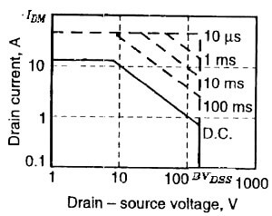
The Safe Operating Area of Power MOSFET is given here:

  • All the maximum voltage and current ratings and power dissipation are conveniently brought together in the safe operating area diagram.
  • This is based on logarithmic plot of drain current against Drain-to-Source voltage as shown in the figure.
  • The solid line shows the bounding values for DC operation.
  • When the MOSFET is operating for a short intervals, the power dissipation is lesser than the continuous operation.
  • So the Power MOSFET Safe Operating Area may be extended as shown in the figure by the dotted line.
  • The factors that determine the SOA of the Power MOSFET arePower MOSFET Safe Operating Area
    1. The maximum drain current IDM
    2. The breakdown voltage BVDSS
    3. The internal junction temperature Tj ( it is governed by the power dissipation in the device)
  • Note that there is no secondary slope on the SOA curves, indicating the absence of second breakdown. We can observe the secondary breakdown problem in BJTs SOA, which is the major drawback or the Power BJT.
  • As the MOSFET does not have second breakdown limit, the Power MOSFET Safe Operating Area (SOA) is large. It means snubber circuits are not required to protect the device in most situations.
  • Because the MOSFET is a majority-carrier device, its on-state resistance has a positive temperature coefficient.
  • If localized and potentially destructive heating occurs within the device the positive temperature coefficient effect of resistance forces local current concentration to be uniformly distributed across the total area.
  • There is no difference between forward-bias and reverse-bias SOAs for the MOSFET. They are identical.
  • The MOSFET will work properly and the device will not degrade when it works within the Safe Operating Limits (SOA) of the device.
  • To select a MOSFET for a particular application, following parameters have to be considered from the device datasheet
    1. Maximum Drain to Source voltage (VDSS)
    2. On-state drain to source resistance RDS(ON)
    3. Drain Current ID
    4. Gate to source Voltage VGS
    5. Reverse recovery time Trr
    6. Gate charge QG
    7. Power Dissipation PD
  • Out of these selection parameters, we can get the limits of maximum drain to source voltage and drain current from the SOA graph of the device.
Don't Miss Our Updates
Be the first to get exclusive content straight to your email.
We promise not to spam you. You can unsubscribe at any time.
Invalid email address
You've successfully subscribed !

Continue Reading

Transistors Questions & Answers
Basics of Ohm’s Law
JFET Working Animation
Laser Diode Working Principle
Full Wave Rectifier
Limitations of Resistors
Share This Article
Facebook Whatsapp Whatsapp LinkedIn Copy Link
Share
Leave a Comment

Leave a Reply Cancel reply

Your email address will not be published. Required fields are marked *

Stay Connected

128.3kFollowersLike
69.1kFollowersFollow
210kSubscribersSubscribe
38kFollowersFollow

Categories

Explore More

Summary Of Transistor Bias Circuits
Zener Diode Voltage Regulator Operation
Different Types of Diodes
Basics of Transistors
Bridge Rectifier Working Animation
Capacitor Filter Operation
Transistor Voltage Divider Bias
Transistor Collector Characteristic Curves

Keep Learning

What is a Filter Circuit

What is a Filter Circuit ?

Short Circuit and Open Circuit

Short Circuit and Open Circuit

Diode-vi-characteristic-curve-for-forward-bias

VI Characteristic of a Diode

How a Multi Color LED Works

How a Multi Color LED Works ?

diode-clamper-circuit

Full Wave Voltage Doubler using Diodes

Short Notes on Rectifiers & Filters

Short Notes on Rectifiers & Filters

Ideal Diode Characteristics

Ideal Diode Characteristics

phototransistor-circuit

Phototransistor Circuit Example

Learn More

Electrical & Instrumentation QA QC Interview Questions

100 Electrical & Instrumentation QA QC Interview Questions

Types of Allen Bradley PLC

Types of Allen Bradley PLC

PID Loop Tuning

PID Controller Loop Tuning Questions and Answers – Part 1

thin-layer chromatography

Thin-Layer Chromatography : Manual Method

Thermocouple measurement and reference junction temperatures

Thermocouple Measurement and Reference Junction Temperatures

AC Generator Operation

Losses in AC Generator

Economics of Power Generation Objective Questions

100+ Economics of Power Generation Objective Questions and Answers

Piping and Instrumentation Diagram

What is Piping and Instrumentation Diagram (P&ID) ?

Menu

  • About
  • Privacy Policy
  • Copyright

Quick Links

  • Learn PLC
  • Helping Hand
  • Part Time Job

YouTube Subscribe

Follow US
All rights reserved. Reproduction in whole or in part without written permission is prohibited.
Welcome Back!

Sign in to your account

Username or Email Address
Password

Lost your password?