Inst ToolsInst ToolsInst Tools
  • Courses
  • Videos
  • Q & A
    • Interview
      • Instrumentation
      • Electronics
      • Electrical
      • Practical Questions
    • MCQ
      • Instrumentation MCQ
      • Electrical MCQ
      • Electronics MCQ
      • Control Systems MCQ
      • Analog Electronics MCQ
      • Digital Electronics MCQ
      • Power Electronics MCQ
      • Microprocessor MCQ
      • Multiple Choice Questions
  • EE
    • Electronics
      • Electronics Q & A
      • Electronic Basics
      • Electronic Devices & Circuits
      • Electronics Animation
      • Digital Electronics
    • Electrical
      • Electrical Basics
      • Electrical Q & A
      • Power Electronics
      • Electrical Machines
      • Electrical Animation
      • Power Systems
      • Switchgear & Protection
      • Transmission & Distribution
  • Measure
    • Control Valves
    • Calibration
    • Temperature
    • Pressure
    • Flow
    • Level
    • Analyzers
    • Switches
    • Vibration
    • Solenoid Valve
  • Control
    • PLC Tutorials
    • Control Systems
    • Safety Instrumented System (SIS)
    • Communication
    • Fire & Gas System
  • More
    • Design
    • Tools
    • Animation
    • Basics
    • Formulas
    • Standards
    • TextBooks
    • Common
    • Software
    • Excel Tools
    • Erection & Commissioning
    • Process Fundamentals
    • Videos
    • Books
Search
All rights reserved. Reproduction in whole or in part without written permission is prohibited.
Reading: PIN Diode Working Principle
Share
Notification Show More
Font ResizerAa
Inst ToolsInst Tools
Font ResizerAa
  • Courses
  • PLC Tutorials
  • Control Systems
Search
  • Courses
  • Videos
  • Q & A
    • Interview
    • MCQ
  • EE
    • Electronics
    • Electrical
  • Measure
    • Control Valves
    • Calibration
    • Temperature
    • Pressure
    • Flow
    • Level
    • Analyzers
    • Switches
    • Vibration
    • Solenoid Valve
  • Control
    • PLC Tutorials
    • Control Systems
    • Safety Instrumented System (SIS)
    • Communication
    • Fire & Gas System
  • More
    • Design
    • Tools
    • Animation
    • Basics
    • Formulas
    • Standards
    • TextBooks
    • Common
    • Software
    • Excel Tools
    • Erection & Commissioning
    • Process Fundamentals
    • Videos
    • Books
Follow US
All rights reserved. Reproduction in whole or in part without written permission is prohibited.
Inst Tools > Blog > Electronic Devices & Circuits > PIN Diode Working Principle

PIN Diode Working Principle

Last updated: September 27, 2016 4:27 pm
Editorial Staff
Electronic Devices & Circuits
No Comments
Share
5 Min Read
SHARE

PIN Diode Working Principle

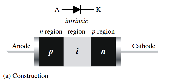
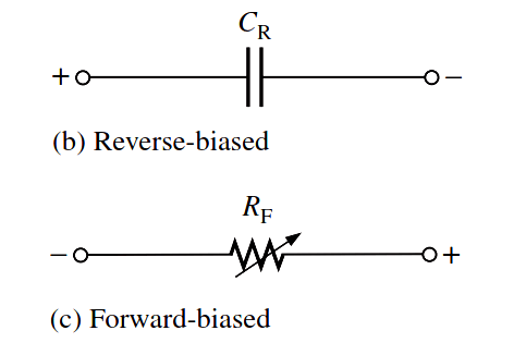
The pin diode consists of heavily doped p and n regions separated by an intrinsic (i) region, as shown in Figure (a). When reverse-biased, the pin diode acts like a nearly constant capacitance. When forward-biased, it acts like a current-controlled variable resistance. This is shown in Figure (b) and (c). The low forward resistance of the intrinsic region decreases with increasing current.

PIN Diode Symbols

The PIN diode operates in exactly the same way as a normal diode. The only real difference is that the depletion region, that normally exists between the P and N regions in an unbiased or reverse biased diode is larger.

In any PN junction, the P region contains holes as it has been doped to ensure that it has a predominance of holes. Similarly the N region has been doped to contain excess electrons. The region between the P and N regions contains no charge carriers as any holes or electrons combine As the depletion region has no charge carriers it acts as an insulator.

PIN Diode

Within a PIN diode the depletion region exists, but if the diode is forward biased, the carriers enter the depletion region (including the intrinsic region) and as the two carrier types meet, current starts to flow.

When the diode is forward biased, the carrier concentration, i.e. holes and electrons is very much higher than the intrinsic level carrier concentration. Due to this high level injection level, the electric field extends deeply (almost the entire length) into the region. This electric field helps in speeding up of the transport of charge carriers from p to n region, which results in faster operation of the diode, making it a suitable device for high frequency operations.

PIN Diode VI Characteristics

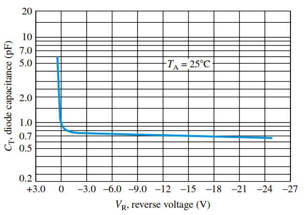
The forward series resistance characteristic and the reverse capacitance characteristic are shown graphically in Below Figure for a typical pin diode. The pin diode is used as a dc-controlled microwave switch operated by rapid changes in bias or as a modulating device that takes advantage of the variable forward-resistance characteristic.

PIN Diode VI Characteristics

Since no rectification occurs at the pn junction, a high-frequency signal can be modulated (varied) by a lower-frequency bias variation. A pin diode can also be used in attenuator applications because its resistance can be controlled by the amount of current. Certain types of pin diodes are used as photodetectors in fiber-optic systems.

pin-diode-vi-characteristics

Advantages of PIN diode

The PIN diode is used in a number of areas as a result of its structure proving some properties which are of particular use.

  • High voltage rectifier:   The PIN diode can be used as a high voltage rectifier. The intrinsic region provides a greater separation between the PN and N regions, allowing higher reverse voltages to be tolerated.
  • RF switch:   The PIN diode makes an ideal RF switch. The intrinsic layer between the P and N regions increases the distance between them. This also decreases the capacitance between them, thereby increasing he level of isolation when the diode is reverse biased.
  • Photodetector:   As the conversion of light into current takes place within the depletion region of a photdiode, increasing the depletion region by adding the intrinsic layer improves the performance by increasing he volume in which light conversion occurs.

These are three of the main applications for PIN diodes, although they can also be used in some other areas as well.

The PIN diode is an ideal component to provide electronics switching in many areas of electronics. It is particularly useful for RF design applications and for providing the switching, or attenuating element in RF switches and RF attenuators. The PIN diode is able to provide much higher levels of reliability than RF relays that are often the only other alternative.

Disadvantages of PIN diode

  • Has a reverse recovery time which contributes to power loss
Don't Miss Our Updates
Be the first to get exclusive content straight to your email.
We promise not to spam you. You can unsubscribe at any time.
Invalid email address
You've successfully subscribed !

Continue Reading

Photodiode as Variable Resistance Device
Positive & Negative Diode Clippers
Basic Transistor Amplifier Circuit Principle
What is Kirchhoff’s Current Law
Full Wave Bridge Rectifier Peak Inverse Voltage
Full Wave Bridge Rectifier Operation
Share This Article
Facebook Whatsapp Whatsapp LinkedIn Copy Link
Share
Leave a Comment

Leave a Reply Cancel reply

Your email address will not be published. Required fields are marked *

Stay Connected

128.3kFollowersLike
69.1kFollowersFollow
208kSubscribersSubscribe
38kFollowersFollow

Categories

Explore More

Comparison of Half wave Rectifiers and Full wave Rectifiers
Difference between Schottky Diode and PN junction Diode
Diode Clampers Principle
Methods of Transistor Biasing
Limitations of Resistors
Diode Limiters/Clippers Operation
Difference between ideal diode & conventional diode
Transistor Cut off, Saturation & Active Regions
Choke Input Filter Operation
Basics of Voltage Regulators

Keep Learning

Shockley Diode Working Principle

Shockley Diode Working Principle

JFET Working Animation

JFET Working Animation

Independent-Voltage-Source-circuit-ideal-battery

Circuit Elements and Types of Circuits

Why Silicon is preferred over Germanium ?

Why Silicon is preferred over Germanium ?

Full Wave Rectifier

Full Wave Rectifier

Diodes Voltage Tripler

Diodes Voltage Tripler

Combining Independent Current Sources in Parallel

Combining Independent Current Sources in Parallel

Power MOSFET Safe Operating Area

Power MOSFET Safe Operating Area

Discover More

Robot Anatomy

Robot – Anatomy, Configuration, Reference Frame, Characteristics

Certified Automation Professional (CAP) Exam Questions

Certified Automation Professional (CAP) Exam Questions

Auto Changeover Switch

What is an Auto Changeover Switch?

PLC XOR LOGIC with Ladder Diagram

PLC Logic Functions

Parking Garage Indicator PLC Automation

Parking Garage Indicator: PLC Automation System

Top 5 Advantages of Human-Machine Interface (HMI)

Top 5 Advantages of Human-Machine Interface (HMI)

What is a Buchholz Relay

What is a Buchholz Relay? Working Principle

Zigbee Projects

Zigbee Based Project Ideas and List

Follow US
All rights reserved. Reproduction in whole or in part without written permission is prohibited.
Welcome Back!

Sign in to your account

Username or Email Address
Password

Lost your password?