Inst ToolsInst ToolsInst Tools
  • Courses
  • Automation
    • PLC
    • Control System
    • Safety System
    • Communication
    • Fire & Gas System
  • Instrumentation
    • Design
    • Pressure
    • Temperature
    • Flow
    • Level
    • Vibration
    • Analyzer
    • Control Valve
    • Switch
    • Calibration
    • Erection & Commissioning
  • Interview
    • Instrumentation
    • Electrical
    • Electronics
    • Practical
  • Q&A
    • Instrumentation
    • Control System
    • Electrical
    • Electronics
    • Analog Electronics
    • Digital Electronics
    • Power Electronics
    • Microprocessor
  • Request
Search
  • Books
  • Software
  • Projects
  • Process
  • Tools
  • Basics
  • Formula
  • Power Plant
  • Root Cause Analysis
  • Electrical Basics
  • Animation
  • Standards
  • 4-20 mA Course
  • Siemens PLC Course
Reading: Bipolar Junction Transistor Construction
Share
Notification Show More
Font ResizerAa
Inst ToolsInst Tools
Font ResizerAa
  • Courses
  • Design
  • PLC
  • Interview
  • Control System
Search
  • Courses
  • Automation
    • PLC
    • Control System
    • Safety System
    • Communication
    • Fire & Gas System
  • Instrumentation
    • Design
    • Pressure
    • Temperature
    • Flow
    • Level
    • Vibration
    • Analyzer
    • Control Valve
    • Switch
    • Calibration
    • Erection & Commissioning
  • Interview
    • Instrumentation
    • Electrical
    • Electronics
    • Practical
  • Q&A
    • Instrumentation
    • Control System
    • Electrical
    • Electronics
    • Analog Electronics
    • Digital Electronics
    • Power Electronics
    • Microprocessor
  • Request
Follow US
All rights reserved. Reproduction in whole or in part without written permission is prohibited.
Inst Tools > Blog > Electronic Devices & Circuits > Bipolar Junction Transistor Construction

Bipolar Junction Transistor Construction

Last updated: September 27, 2016 4:17 pm
Editorial Staff
Electronic Devices & Circuits
No Comments
Share
2 Min Read
SHARE

The basic structure of the bipolar junction transistor (BJT) determines its operating characteristics.

The BJT is constructed with three doped semiconductor regions separated by two pn junctions, as shown in the epitaxial planar structure in Figure (a). The three regions are called emitter, base, and collector. Physical representations of the two types of BJTs are shown in Figure (b) and (c). One type consists of two n regions separated by a p region (npn), and the other type consists of two p regions separated by an n region (pnp). The term bipolar refers to the use of both holes and electrons as current carriers in the transistor structure.

Bipolar Junction Transistor Construction

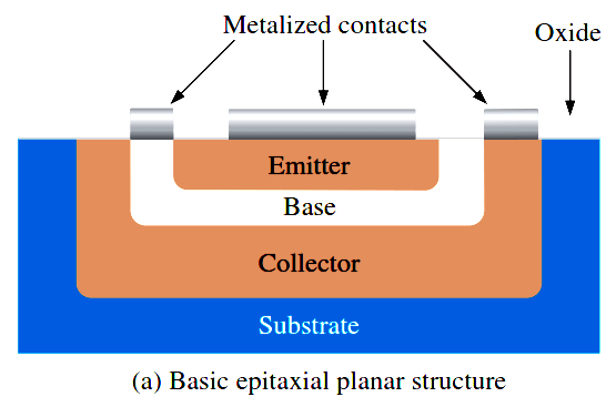
Fig : Basic BJT construction.

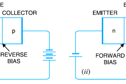
The pn junction joining the base region and the emitter region is called the base-emitter junction. The pn junction joining the base region and the collector region is called the base-collector junction, as indicated in Above Figure (b). A wire lead connects to each of the three regions, as shown. These leads are labeled E, B, and C for emitter, base, and collector, respectively.

bipolar-junction-transistor-symbol

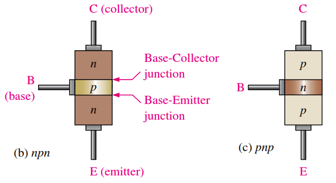
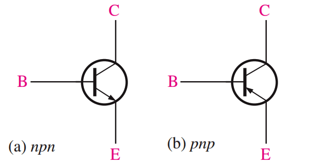
The base region is lightly doped and very thin compared to the heavily doped emitter and the moderately doped collector regions. The Below  Figure shows the schematic symbols for the npn and pnp bipolar junction transistors.

bjt-bipolar-junction-transistor-symbols

Don't Miss Our Updates
Be the first to get exclusive content straight to your email.
We promise not to spam you. You can unsubscribe at any time.
Invalid email address
You've successfully subscribed !

Continue Reading

Transistor Collector Feedback Bias
Why Silicon is preferred over Germanium ?
Dependent Current Source
Capacitor Filter Operation
Center Tapped Full Wave Rectifier Operation
CRT Fluorescent Screen
Share This Article
Facebook Whatsapp Whatsapp LinkedIn Copy Link
Share
Leave a Comment

Leave a Reply Cancel reply

Your email address will not be published. Required fields are marked *

Stay Connected

128.3kFollowersLike
69.1kFollowersFollow
210kSubscribersSubscribe
38kFollowersFollow

Categories

Explore More

Difference between Schottky Diode and PN junction Diode
Shockley Diode Working Principle
What is a Filter Circuit ?
Resistors Principle & Applications
Transistor Voltage Divider Bias
Operation of Zener Diode Voltage Regulator
Different Types of Diodes
What is Kirchhoff’s Current Law

Keep Learning

diode-clamper-circuit

Full Wave Voltage Doubler using Diodes

Independent-Voltage-Source-circuit-ideal-battery

Circuit Elements and Types of Circuits

kirchhoffs-voltage-law

What is Kirchhoff’s Voltage Law

Reverse Voltage Characteristics of Photo diode

Characteristics of Photo diode

parallel-resistors-circuit-example

Series and Parallel Resistors

Transistor Collector Characteristic Curves

Transistor Collector Characteristic Curves

half-wave-voltage-doubler-using-diodes

Half Wave Voltage Doubler using Diodes

pn-junction-energy-diagrams

Energy Diagrams of PN Junction & Depletion Region

Learn More

Reed Switch Principle

Reed switch Working Principle

Pneumatic-Level-Transmitter-Value-Struck

Pneumatic Level Transmitter Value Struck?

Electrical Machines Questions and Answers

Transformer Losses and Efficiency

Programmable Logic Controller (PLC) Questions and Answers

Programmable Logic Controller (PLC) Questions and Answers – 2

List of 100 Sensors and Transducers Questions

List of 100 Sensors and Transducers Questions

Electromagnetic Fields Objective Questions

Electromagnetic Field MCQ

PLC based Automatic Packaging System

PLC based Automatic Packaging System

Temperature and Humidity Objective Questions

Temperature and Humidity Objective Questions

Menu

  • About
  • Privacy Policy
  • Copyright

Quick Links

  • Learn PLC
  • Helping Hand
  • Part Time Job

YouTube Subscribe

Follow US
All rights reserved. Reproduction in whole or in part without written permission is prohibited.
Welcome Back!

Sign in to your account

Username or Email Address
Password

Lost your password?