Inst ToolsInst ToolsInst Tools
  • Ask
  • Courses
  • Videos
  • Q & A
    • Interview
      • Instrumentation
      • Electronics
      • Electrical
      • Practical Questions
    • MCQ
      • Instrumentation MCQ
      • Electrical MCQ
      • Electronics MCQ
      • Control Systems MCQ
      • Analog Electronics MCQ
      • Digital Electronics MCQ
      • Power Electronics MCQ
      • Microprocessor MCQ
      • Multiple Choice Questions
  • EE
    • Electronics
      • Electronics Q & A
      • Electronic Basics
      • Electronic Devices & Circuits
      • Electronics Animation
      • Digital Electronics
    • Electrical
      • Electrical Basics
      • Electrical Q & A
      • Power Electronics
      • Electrical Machines
      • Electrical Animation
      • Power Systems
      • Switchgear & Protection
      • Transmission & Distribution
  • Measure
    • Control Valves
    • Calibration
    • Temperature
    • Pressure
    • Flow
    • Level
    • Analyzers
    • Switches
    • Vibration
    • Solenoid Valve
  • Control
    • PLC Tutorials
    • Control Systems
    • Safety Instrumented System (SIS)
    • Communication
    • Fire & Gas System
  • More
    • Design
    • Tools
    • Animation
    • Basics
    • Formulas
    • Standards
    • TextBooks
    • Common
    • Software
    • Excel Tools
    • Erection & Commissioning
    • Process Fundamentals
    • Videos
    • Books
Search
All rights reserved. Reproduction in whole or in part without written permission is prohibited.
Reading: Energy Diagrams of PN Junction & Depletion Region
Share
Notification Show More
Font ResizerAa
Inst ToolsInst Tools
Font ResizerAa
  • Courses
  • PLC Tutorials
  • Control Systems
Search
  • Ask
  • Courses
  • Videos
  • Q & A
    • Interview
    • MCQ
  • EE
    • Electronics
    • Electrical
  • Measure
    • Control Valves
    • Calibration
    • Temperature
    • Pressure
    • Flow
    • Level
    • Analyzers
    • Switches
    • Vibration
    • Solenoid Valve
  • Control
    • PLC Tutorials
    • Control Systems
    • Safety Instrumented System (SIS)
    • Communication
    • Fire & Gas System
  • More
    • Design
    • Tools
    • Animation
    • Basics
    • Formulas
    • Standards
    • TextBooks
    • Common
    • Software
    • Excel Tools
    • Erection & Commissioning
    • Process Fundamentals
    • Videos
    • Books
Follow US
All rights reserved. Reproduction in whole or in part without written permission is prohibited.
Inst Tools > Blog > Electronic Devices & Circuits > Energy Diagrams of PN Junction & Depletion Region

Energy Diagrams of PN Junction & Depletion Region

Last updated: October 5, 2016 1:19 pm
Editorial Staff
Electronic Devices & Circuits
2 Comments
Share
3 Min Read
SHARE

The valence and conduction bands in an n-type material are at slightly lower energy levels than the valence and conduction bands in a p-type material. Recall that p-type material has trivalent impurities and n-type material has pentavalent impurities. The trivalent impurities exert lower forces on the outer-shell electrons than the pentavalent impurities. The lower forces in p-type materials mean that the electron orbits are slightly larger and hence have greater energy than the electron orbits in the n-type materials.

An energy diagram for a pn junction at the instant of formation is shown in Figure (a). As you can see, the valence and conduction bands in the n region are at lower energy levels than those in the p region, but there is a significant amount of overlapping.

Energy-diagrams-of-the-pn-junction-and-depletion-region

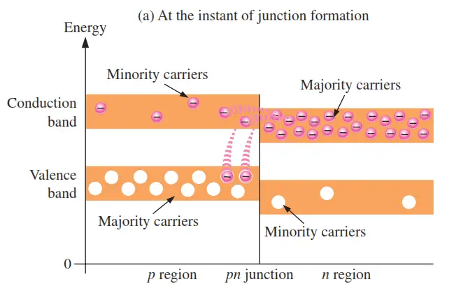
The free electrons in the n region that occupy the upper part of the conduction band in terms of their energy can easily diffuse across the junction (they do not have to gain additional energy) and temporarily become free electrons in the lower part of the p-region conduction band. After crossing the junction, the electrons quickly lose energy and fall into the holes in the p-region valence band as indicated in Figure (a).

As the diffusion continues, the depletion region begins to form and the energy level of the n-region conduction band decreases. The decrease in the energy level of the conduction band in the n region is due to the loss of the higher nergy electrons that have diffused across the junction to the p region. Soon, there are no electrons left in the n-region conduction band with enough energy to get across the junction to the p-region conduction band, as indicated by the alignment of the top of the n-region conduction band and the bottom of the p-region conduction band in Figure (b). At this point, the junction is at equilibrium; and the depletion region is complete because diffusion has ceased. There is an energy gradiant across the depletion region which acts as an “energy hill” that an n-region electron must climb to get to the p region.

pn-junction-energy-diagrams

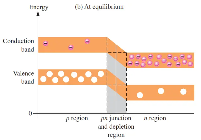
Notice that as the energy level of the n-region conduction band has shifted downward, the energy level of the valence band has also shifted downward. It still takes the same amount of energy for a valence electron to become a free electron. In other words, the energy gap between the valence band and the conduction band remains the same.

Don't Miss Our Updates
Be the first to get exclusive content straight to your email.
We promise not to spam you. You can unsubscribe at any time.
Invalid email address
You've successfully subscribed !
Optocouplers Working Principle
Voltage Divider Rule
Comparison of Half wave Rectifiers and Full wave Rectifiers
Combining Independent Current Sources in Parallel
What is a Memristor? Principle, Advantages, Applications
Share This Article
Facebook Whatsapp Whatsapp LinkedIn Copy Link
Share
2 Comments
  • Kisore says:
    July 22, 2021 at 11:30 am

    Now i could understand clearly. Tq

    Reply
  • Matt says:
    September 27, 2022 at 9:05 pm

    How does the higher energy electrons diffuse to the p-side from the CB of n-side shift the fermi level down?

    Reply

Leave a Reply Cancel reply

Your email address will not be published. Required fields are marked *

Stay Connected

128.3kFollowersLike
69.1kFollowersFollow
208kSubscribersSubscribe
38kFollowersFollow

Categories

Recent Comments

  • Kamli on Top Free PLC Software
  • Guifty Shimica on Top Non-PLC Certification Courses for Automation Professionals
  • Guifty Shimica on Top Non-PLC Certification Courses for Automation Professionals
  • MIHARITSOA Aina Sitraka on Top Non-PLC Certification Courses for Automation Professionals

Related Articles

Transistor Biasing

Transistor Biasing

Troubleshooting a Biased Transistor

Troubleshooting a Biased Transistor

Transistor Amplifier Working Principle

Diode-testing-with-multimeter

How to Test a Diode using Multimeter

Transistor Collector Characteristic Curves

Transistor Collector Characteristic Curves

Combining Independent Voltage Sources in Series

Combining Independent Voltage Sources in Series

Reverse Voltage Characteristics of Photo diode

Characteristics of Photo diode

Field Instruments Questions and Answers

Basics of Amplifiers Interview Questions

More Articles

Instrumentation and Control Engineering Questions and Answers

Instrumentation and Control Engineering Questions and Answers

DC motor speed control

DC Motor Speed Control

Functional block diagram for analog alarms

PLC Logic for Analog Alarms using Functional Block Diagram

Digital Electronics Multiple Choice Questions

Hardware Description Language Objective Questions

Chlorine Cylinders

Chlorine Gas Hazards

Loop Diagram

Documentation and Change Control of PLC or DCS Systems

Seven Segment Display Programming with Structured Text

Seven Segment Display Programming with Structured Text

FBD Logic

Why different PLC Programming Languages were Developed?

Follow US
All rights reserved. Reproduction in whole or in part without written permission is prohibited.
Welcome Back!

Sign in to your account

Username or Email Address
Password

Lost your password?