Rectifiers
Most electrical power generating stations produce alternating current. The major reason for generating AC is that it can be transferred over long distances with fewer losses than DC; however, many of the devices which are used today operate only, or more efficiently, with DC. For example, transistors, electron tubes, and certain electronic control devices require DC for operation. If we are to operate these devices from ordinary AC outlet receptacles, they must be equipped with rectifier units to convert AC to DC. In order to accomplish this conversion, we use diodes in rectifier circuits.
The purpose of a rectifier circuit is to convert AC power to DC. The most common type of solid state diode rectifier is made of silicon. The diode acts as a gate, which allows current to pass in one direction and blocks current in the other direction. The polarity of the applied voltage determines if the diode will conduct. The two polarities are known as forward bias and reverse bias.
Forward Bias
A diode is forward biased when the positive terminal of a voltage source is connected to its anode, and the negative terminal is connected to the cathode (Figure 4A). The power source’s positive side will tend to repel the holes in the p-type material toward the p-n junction by the negative side. A hole is a vacancy in the electron structure of a material. Holes behave as positive charges. As the holes and the electrons reach the p-n junction, some of them break through it (Figure 4B). Holes combine with electrons in the n-type material, and electrons combine with holes in the p-type material.
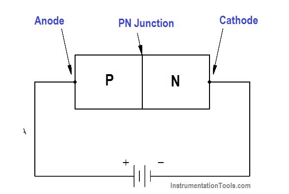
Figure 4 A – Forward-Biased Diode
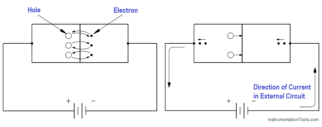
Figure 4B (Left) & 4C (Right)
When a hole combines with an electron, or an electron combines with a hole near the p-n junction, an electron from an electron-pair bond in the p-type material breaks its bond and enters the positive side of the source. Simultaneously, an electron from the negative side of the source enters the n-type material (Figure 4C). This produces a flow of electrons in the circuit.
Reverse Bias
Reverse biasing occurs when the diode’s anode is connected to the negative side of the source, and the cathode is connected to the positive side of the source (Figure 5A). Holes within the p-type material are attracted toward the negative terminal, and the electrons in the n-type material are attracted to the positive terminal (Figure 5B). This prevents the combination of electrons and holes near the p-n junction, and therefore causes a high resistance to current flow. This resistance prevents current flow through the circuit.
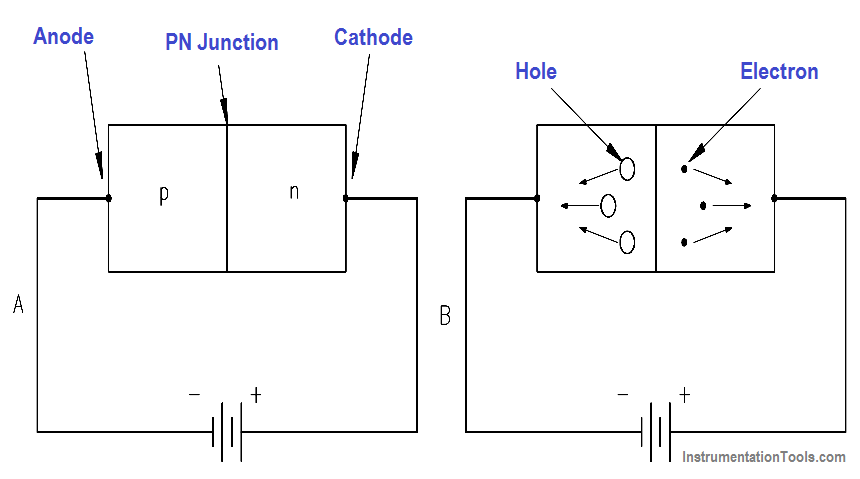
Figure 5 Reverse-Biased Diode