Inst ToolsInst ToolsInst Tools
  • Courses
  • Automation
    • PLC
    • Control System
    • Safety System
    • Communication
    • Fire & Gas System
  • Instrumentation
    • Design
    • Pressure
    • Temperature
    • Flow
    • Level
    • Vibration
    • Analyzer
    • Control Valve
    • Switch
    • Calibration
    • Erection & Commissioning
  • Interview
    • Instrumentation
    • Electrical
    • Electronics
    • Practical
  • Q&A
    • Instrumentation
    • Control System
    • Electrical
    • Electronics
    • Analog Electronics
    • Digital Electronics
    • Power Electronics
    • Microprocessor
  • Request
Search
  • Books
  • Software
  • Projects
  • Process
  • Tools
  • Basics
  • Formula
  • Power Plant
  • Root Cause Analysis
  • Electrical Basics
  • Animation
  • Standards
  • 4-20 mA Course
  • Siemens PLC Course
Reading: Energy Diagrams of PN Junction & Depletion Region
Share
Font ResizerAa
Inst ToolsInst Tools
Font ResizerAa
  • Courses
  • Design
  • PLC
  • Interview
  • Control System
Search
  • Courses
  • Automation
    • PLC
    • Control System
    • Safety System
    • Communication
    • Fire & Gas System
  • Instrumentation
    • Design
    • Pressure
    • Temperature
    • Flow
    • Level
    • Vibration
    • Analyzer
    • Control Valve
    • Switch
    • Calibration
    • Erection & Commissioning
  • Interview
    • Instrumentation
    • Electrical
    • Electronics
    • Practical
  • Q&A
    • Instrumentation
    • Control System
    • Electrical
    • Electronics
    • Analog Electronics
    • Digital Electronics
    • Power Electronics
    • Microprocessor
  • Request
Follow US
All rights reserved. Reproduction in whole or in part without written permission is prohibited.
Inst Tools > Blog > Electronic Devices & Circuits > Energy Diagrams of PN Junction & Depletion Region

Energy Diagrams of PN Junction & Depletion Region

Last updated: October 5, 2016 1:19 pm
Editorial Staff
Electronic Devices & Circuits
2 Comments
Share
3 Min Read
SHARE

The valence and conduction bands in an n-type material are at slightly lower energy levels than the valence and conduction bands in a p-type material. Recall that p-type material has trivalent impurities and n-type material has pentavalent impurities. The trivalent impurities exert lower forces on the outer-shell electrons than the pentavalent impurities. The lower forces in p-type materials mean that the electron orbits are slightly larger and hence have greater energy than the electron orbits in the n-type materials.

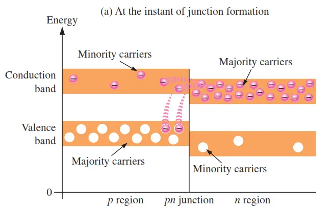
An energy diagram for a pn junction at the instant of formation is shown in Figure (a). As you can see, the valence and conduction bands in the n region are at lower energy levels than those in the p region, but there is a significant amount of overlapping.

Energy-diagrams-of-the-pn-junction-and-depletion-region

The free electrons in the n region that occupy the upper part of the conduction band in terms of their energy can easily diffuse across the junction (they do not have to gain additional energy) and temporarily become free electrons in the lower part of the p-region conduction band. After crossing the junction, the electrons quickly lose energy and fall into the holes in the p-region valence band as indicated in Figure (a).

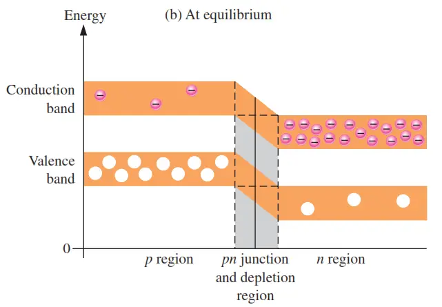
As the diffusion continues, the depletion region begins to form and the energy level of the n-region conduction band decreases. The decrease in the energy level of the conduction band in the n region is due to the loss of the higher nergy electrons that have diffused across the junction to the p region. Soon, there are no electrons left in the n-region conduction band with enough energy to get across the junction to the p-region conduction band, as indicated by the alignment of the top of the n-region conduction band and the bottom of the p-region conduction band in Figure (b). At this point, the junction is at equilibrium; and the depletion region is complete because diffusion has ceased. There is an energy gradiant across the depletion region which acts as an “energy hill” that an n-region electron must climb to get to the p region.

pn-junction-energy-diagrams

Notice that as the energy level of the n-region conduction band has shifted downward, the energy level of the valence band has also shifted downward. It still takes the same amount of energy for a valence electron to become a free electron. In other words, the energy gap between the valence band and the conduction band remains the same.
Don't Miss Our Updates
Be the first to get exclusive content straight to your email.
We promise not to spam you. You can unsubscribe at any time.
Invalid email address
You've successfully subscribed !

Continue Reading

Transistor Base Bias
Short Circuit and Open Circuit
Phototransistor Working Principle
Shockley Diode Working Principle
Transistor Amplifier Working Principle
Full Wave Voltage Doubler using Diodes
Share This Article
Facebook Whatsapp Whatsapp LinkedIn Copy Link
Share
2 Comments
  • Kisore says:
    July 22, 2021 at 11:30 am

    Now i could understand clearly. Tq

    Reply
  • Matt says:
    September 27, 2022 at 9:05 pm

    How does the higher energy electrons diffuse to the p-side from the CB of n-side shift the fermi level down?

    Reply

Leave a Reply Cancel reply

Your email address will not be published. Required fields are marked *

Stay Connected

128.3kFollowersLike
69.1kFollowersFollow
210kSubscribersSubscribe
38kFollowersFollow

Categories

Explore More

Varactor Diode Operation
Transistor Collector Characteristic Curves
Power MOSFET Safe Operating Area
Capacitor Filter Operation
Zener Diode Voltage Regulator Operation
VI Characteristic of a Diode
Transistors Questions & Answers
Transistor as an Amplifier in Common Emitter

Keep Learning

Fluorescent Screen of CRT

CRT Fluorescent Screen

Zener Diode Limiter Working

Zener Diode Limiter

Types-of-diodes

Different Types of Diodes

full-wave-bridge-rectifier-with-voltage-regulator

Basics of Voltage Regulators

basic-electronics-questions-answers

Basic Electronics Questions & Answers

half-wave-voltage-doubler-using-diodes

Half Wave Voltage Doubler using Diodes

Cathode Ray Tube Deflection System

Cathode Ray Tube Deflection System

Diode-positive-limiter

Positive & Negative Diode Clippers

Learn More

toroidal conductivity probe principle

Electrodeless Conductivity Probes Principle

Oscillating Piston Flow Meters Principle Animation

Nutating Disc Flow Meters Working Principle

Rotary Granulator Drive

Rotary Granulator Drive Root Cause Analysis (RCA)

Special Purpose Diodes Interview Questions & Answers

Special Purpose Diodes Interview Questions & Answers

PLC control 4 machines with 1 button

CX-Programmer Tutorial: 1 Button To Activate 4 Different Machines

PLC based Automatic Bell System

PLC based Automatic Bell System for a School

Wedge Flow Meter

Wedge Flow Meter Principle

Integral Control Principle

Integral Controller Principle

Menu

  • About
  • Privacy Policy
  • Copyright

Quick Links

  • Learn PLC
  • Helping Hand
  • Part Time Job

YouTube Subscribe

Follow US
All rights reserved. Reproduction in whole or in part without written permission is prohibited.
Welcome Back!

Sign in to your account

Username or Email Address
Password

Lost your password?