Thin film deposition systems are an essential part of the manufacturing process. Products ranging from smartphones to solar panels would not exist without thin film deposition. While these systems have an integral role in materials science, their function and operation can be quite complicated.
There are various deposition techniques and even more configurations for thin film deposition systems. Each technique, some of which we cover below, has its own advantages for application.
In this overview, we will discuss how thin film deposition works and how each system completes deposition.
What is a Thin Film Deposition System?
The thin-film deposition is a vital part of the electronics manufacturing process. These systems are, in part, responsible for the creation of diodes, microprocessors, and transistors.
A thin film deposition system is a tool for those working in materials science to deposit thin film coatings onto various materials.
Made from materials such as metals or oxides, thin film deposition systems place a thin layer of atoms onto substrates (usually silicon wafers) during the assembly process. These systems are essential to producing semiconductor and fibre lasers, consumer electronics, and many types of medical implants.
Depending on a user’s requirements, there are different systems and methods of thin film deposition. With a tool like Korvus Technology’s Hex series system, users have access to different deposition systems and tools. Thin film deposition applications are boundless, including:
- Contact metallisation
- EM sample preparation
- Sputter deposition
- Research of new coatings
The Hex series allows for state-of-the-art deposition and analysis focused on students’ needs with multiple, interchangeable configurations.
Different products and projects require different systems and techniques of thin film deposition.
How Does a Thin Film Deposition System Work?
The thin-film deposition is either chemical deposition or physical deposition. Different thin film deposition systems have their own processes and applications.
Depending on the chemical reaction taking place, chemical deposition breaks down into additional categories, such as chemical vapour deposition and atomic layer deposition (ALD).
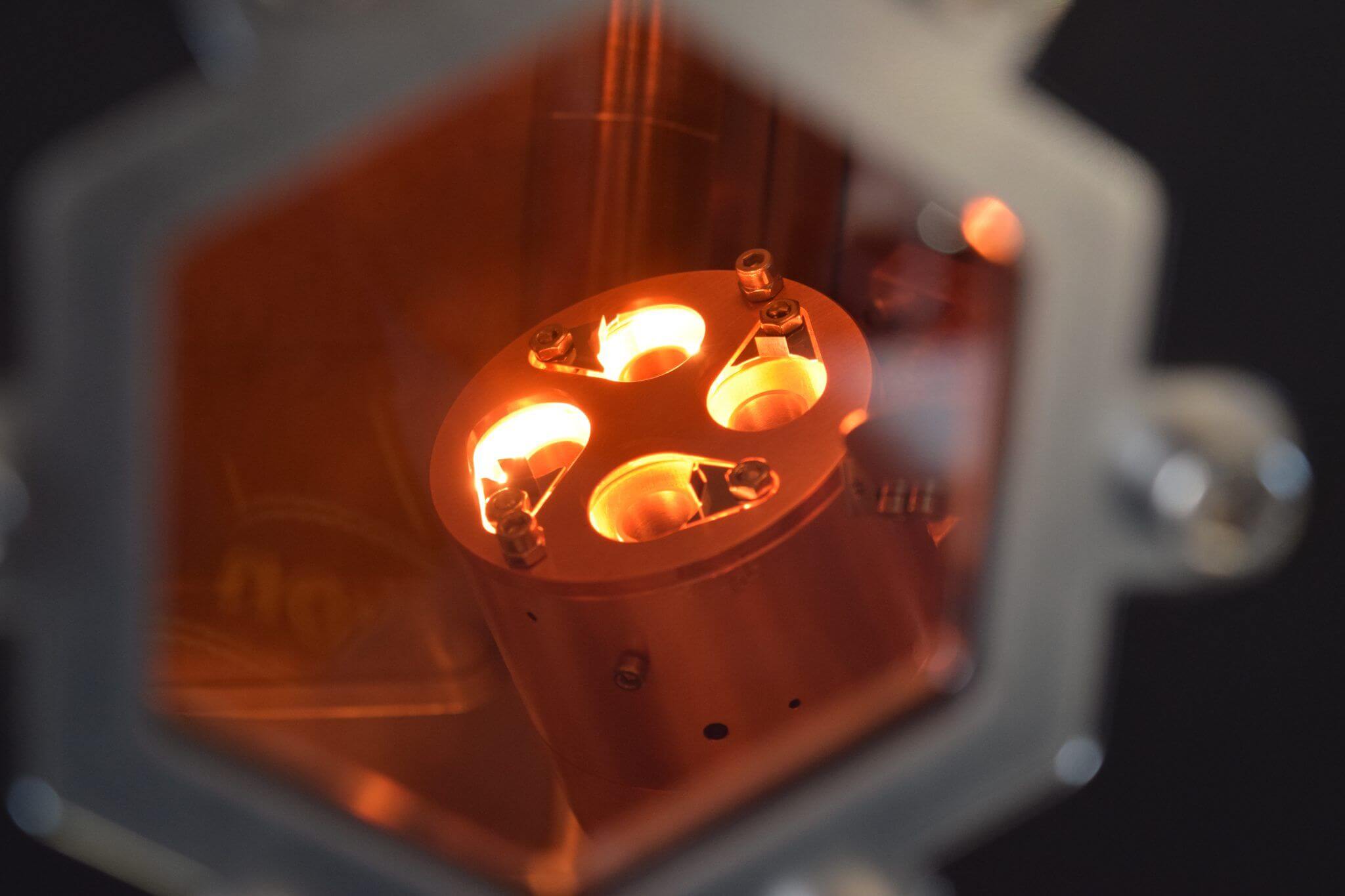
In a physical deposition process known as physical vapour deposition, which we discuss below, high-energy techniques vaporize solid materials in a vacuum for deposition onto a target material.
Two methods of PVD include sputtering and evaporation.
Magnetron Sputtering
Magnetron sputtering is a plasma-based physical vapour deposition method. Plasma ions interact with the material and cause atoms to sputter, or spray, which creates the thin film on the substrate.
This is how thin film deposition works in most electrical or optical production settings.
E-beam Evaporation
E-beam evaporation uses a high-energy electron beam evaporator to evaporate the material. This vapour then creates a thin film for deposition. This method is commonly used for solar panels and glass.
Thermal Evaporation
Another evaporation method, thermal evaporation is a simple form of physical vapour deposition. This method creates a reaction through extreme heat to vaporize the target material.
Thermal evaporation is useful for creating OLEDS and thin-film transistors.
Final Thoughts
Many of the technologies we use every day would not exist without thin film deposition. Knowing these systems and how thin film deposition works is the first step towards choosing the most appropriate method for any project. Explore other blog posts to learn more about thin film deposition systems and the revolutionary HEX series by Korvus Technology.