1) What is an Electric Potential?
The potential of a particular point, is defined as the work done to move a positive charge particle to move to that point in opposite to electric field. It may be an external energy applied to move that positive charge or may be internal potential energy of the positive charge.
2) What is Potential Difference?
The differential in potentials at two points in an electric field is called as potential difference between two points. It is measure in Volts i.e. VAB is called the potential difference between points A & B. If the VAB is positive then it illustrates that the potential at point A is high compared to potential at point B. In this case there will be chance of movement of charged particle from A to B against to electrical field between the points.
VAB = VA – VB
3) What is a Transit time of an Electron?
The time taken by an electron to travel from one electrode to the other electrode is called electron transit time. It is denoted as ‘τ’.
Where V = Potential applied to electron
d= Distance between electrodes
e = Electron charge
m = mass of an electron
Note: The transit time of an electron decreases with the increase in potential (V).
4) What is an Electron Volt(eV)?
One Electron volt is the energy gained by the electron when it falls from one point to another point which has a potential difference of 1 volt. I.e. under potential difference of one volt, the electron moves from higher potential to lower potential, during this free fall in the electron field it gains an electron volt energy.
In other case it the energy required to move an electron in the potential difference of one volt. This is against to the electric field.
5) What is an Electric Field intensity(ε)?
6) What is an Ionization Potential?
The energy required to detach an loosely coupled electron from the influence of parent nucleus is called ionization potential.
7) What is an electron spin?
The electron generally orbits around the parent nucleus and in addition to this it also rotates around itself like an earth. This intrinsic angular momentum property of en electron is called electron spin. There are only two direction of spins when it is subjected to a magnetic field i.e. either parallel or anti-parallel to the field.
8) What is N type Semiconductor?
When extra valance electrons are introduced in a pure semi-conductor material (silicon) by putting or injecting dopants or impurities, an N-type material is produced. The dopants are used to create an N-Type material are Group-V elements in the materials table.
- N-type semiconductor bond diagram
Group V elements: Arsenic, antimony, phosphorus.
In N-type semiconductor electrons are majority carriers and holes are minority carriers.
9) What is P- Type Semiconductor?
When a dopant from Group III elements from the elements table is introduced in to pure semiconductor, produces a P-Type semiconductor. The Group III elements have only 3 valance electrons in its outer orbit which there combines with four valance electrons semiconductor material (silicon). This results in missing of electron which creates a hole (P+) , or positive charge that can freely move around in the material.
- P-type semiconductor bond diagram
Group III elements: aluminum, boron, and gallium.
In P-Type semiconductor, holes are the majority carriers and electrons are the minority carriers.
10) What are passive and active components?
Passive components: The components which are passive in nature i.e. which can attenuate the input applied signal to a desired level. These are energy consumers and cannot boost the input signal. Resistors, capacitors and inductors are the examples of passive components.
Active components: The components which plays an active role in the electronic circuit i.e. which can add energy to the input signal are called active components. These can amplify the signal to the desired level. Transistors, operational amplifiers are the examples of active components.
What are conductors,insulators and semiconductors?
Conductors: The materials which permits the flow of charge carriers with higher conductivity are called conductors. In conductor, the valance band and conduction band overlaps with out any energy gap(EG). The conductivity of a conductor is normally greater than 103. The examples of conductors are gold, silver, copper etc.
Insulators: The materials which blocks the flow of electrons or which offers higher resistivity to the flow of electrons are called insulators. The energy gap between valency and conduction bad in the insulators is greater than 1eV. The conductivity of insulator is less than 10-7 and the examples of insulators are rubber, glass, Teflon, mica etc.
Semiconductors: The materials which are partially conductive and whose conductivity can be controlled are called semiconductors. These are most useful materials in electronic circuits. The energy gap Eg between valency and conduction bad of semiconductors are almost equal to 1eV. Silicon and Germanium are the best examples of semiconductors.
What are the advantages of silicon over germanium?
Advantages:
- Easily available in nature.
- Cost is low compared to germanium
- Higher temperature operating ranges compared to germanium.
- Wider band gap than germinum
- Less noisy compared to germanium
- The material properties are accurately controlled
What are the advantages and disadvantages of semiconductor over other devices?
Advantages:
- These are smaller in size
- Long life compared to vacuum tubes.
- Operated on low DC power
- Accuracy is high compared to vacuum tubes
- Noise is less
- Warm up is not needed in semiconductors.
Disadvantages:
- Cannot withstand for high power.
- Frequency range of operation is low.
- produces less output power.
- Accuracy changes with the temperature.
- Low ambient temperature.
What is a mobility of a charge carrier?
The mobility of a charge carrier is the velocity per unit electri field. It is enoted as μ and its units are m2/v-sec.
Note: As the temperature increases the mobility of charge carrier decreases because of the random motion of charge carriers.
What is mass action law and law of electrical neutrality?
Mass Action law: It states that in an intrinsic semiconductor the product of free electrons ‘n’ and free holes ‘p’ is constant. I.e.
np = ni2
Law of electrical neutrality: It states that when no voltage is applied to semiconductor, the magnitude of positive charge density must equals that of negative charge density.
Total positive charge density = ND+p
Total negitive charge density = NA+p
i.e.
ND + P=NA + n
Where ND and NA are donor and acceptor densities.
What is an Electric Potential?
Electric potential of a system of charged particles at a point P is defined as work done in moving those charges from reference point to point P divided by total charge of system of particles. The reference point is generally taken to be infinity or some large chunk of neutral body such as earth.
(Or)
Electric potential at a point P is defined as the work done in moving unit coulomb charge from infinity point free of electric fields to point P. Electric potential is measured in terms of volts. It is also called absolute potential and is denoted by V. It is a scalar quantity. Electric potential of a point varies with the choice of reference point w.r.t which potential is measured.
Electric potential Va = W/Σq
What is Potential Difference?
Potential difference between two points A and B is defined as work done in moving one coulomb charge from point A to B. Alternatively it is understood to be difference of absolute potential of point A and B. It is denoted by VAB. If VAand VB are the electric potentials at points A and B with respect to common reference point (mostly this is taken to be ground i.e. ground is assumed to be at zero potential) then the potential difference between points A and B is given by
VAB = VA – VB
Potential difference between points is invariant w.r.t the choice of reference point.
What is a Transit time of an Electron between two electrodes?
It is the time taken for an electrode to travel from one electrode to another. Electron since a negatively charge particle travels from low potential to high potential in the direction opposite the electric field direction. Assume a uniform electric field E between two electrodes with spacing between them equal to dthen the transit time of electron is given by
T = (
)
where m and q are mass and charge of electron.
What is an Electron Volt eV?
It is the defined as the work done in moving an electron through a potential difference of one volt. Typically all the energies involving electron are specified in electron volts for simplicity and ease in analyzing. One electron volt is equal to 1.6*10-19 joules. It can be deduced as follows, the work done in moving a charged particle with charge q from point A to point B whose potentials w.r.t. ground are VA and VB is given by
W = q*( VA – VB), with q=1.6*10-19 coulomb and VA – VB = 1 volt this reduces to 1.6*10-19 J which by definition is electron volt.
What is Electric Field intensity (ε)?
Electric field intensity at a point p in space is defined as the force acting on a unit charge particle with the assumption that the unit charge should not disturb the electric field itself but normally that is the case as one coulomb of charge includes 6.25*1018 charged particles with each particle carrying electronic charge i.e. 1.6*10-19 coulombs.
So the test charge used to measure the field should be as small as possible (Note: the smallest charge stable charge in nature is of electron’s).Hence theoretically electric field is defined as force acting on a test charge divided by the test charge itself as the charge tends to zero.
E = F/q as q–>0 C
It is a vector quantity and always starts from positive charge and ends on negative charge.
What is an Ionization Potential?
The minimum amount of energy required to remove an electron from an isolated atom or molecule is termed as Ionization potential. It is specified in units of electron volts. Example for Hydrogen atom the ionization potential is 13.6 eV.
What is an electron spin?
An electron in an atom while revolving around the nuclei of atom rotates around itself. The spin of electron is assigned a quantum number known as spin quantum number which can take values of +1/2 and -1/2 for clockwise and anticlockwise rotation.
What is an extrinsic semiconductor?
Intrinsic semiconductor like pure silicon and germanium are characterized by high resistivity because of low free carrier charge density e.t.c. Hence in order to increase conductivity trivalent and pentavalent impurities are added. The added impurities are called dopants and the process is termed as doping. The resulting semiconductor after doping is called extrinsic semiconductor.
What is N type Semiconductor?
If the dopant added to an intrinsic semiconductor is a pentavalent impurity such as phosphorous, Arsenic, Antimony the resulting semiconductor is termed as N-type conductor. The added impurity atoms will displace some of silicon atoms in the crystal lattice. Four of the valence electrons of dopant will occupy covalent bonds with silicon; fifth electron will be nominally free and can be used as carrier of current. The energy required to detach this fifth electron is of the order of 0.01eV for Germanium and 0.05eV for Silicon.
This can be understood alternatively as follows, due to replacement of some of the silicon atoms with pentavalent atoms from the crystal the energy band structure of the crystal lattice gets altered. The consequence of this alteration is the introduction of new allowable energy levels in the band structure in the forbidden gap close to conduction band. The energy required to excite the electrons occupying this new energy level to conduction band is of the order of 0.01 eV for Germanium and 0.05 for Silicon.
What is P- Type Semiconductor?
If the dopant added to an intrinsic semiconductor is a trivalent impurity such as Boron, Indium, Gallium the resulting semiconductor is termed as P-type conductor. The added impurity atoms will displace some of silicon atoms in the crystal lattice. Three of the valence electrons of dopant will occupy covalent bonds with silicon; vacancy in the fourth bond constitutes a hole which effectively acts as positive charge carrier and can accept an electron.
Due to replacement of some of the silicon atoms with trivalent atoms from the crystal the energy band structure of the crystal lattice gets altered. The consequence of this alteration is the introduction of new allowable energy levels in the band structure in the forbidden gap close to valence band. The energy required to excite the electrons from valence band to this new energy level is of the order of 0.01 eV for Ge and 0.05 for Si generating holes in valence band.
What are passive and active elements?
Active component is one which is capable of delivering energy independently. Examples are voltage and current sources, transistors, Opamp e.t.c. If the element is not capable of delivering energy then it is termed as Passive element.
Bohr’s model?
Bohr’s model is one of the proposed model of atom and was able to explain the emission and absorption spectra of hydrogen and single electron ions such as He2+. Some of the main postulates of Bohr’s atomic model are:
a) Electrons revolve around the nucleus of atom much like planets revolve around the sun in only definite circular paths called as orbits. Each orbit corresponds to a definite energy. The energy values are quantized and are allowed to posses only certain values.
b) As long as the electron is in this path it will not absorb or emit radiation and the atom will be stable. Hence these are called stationary orbits.When an electron drops from higher energy orbit to lower energy orbit, the difference in the energy of those orbits will be emitted as radiation.
where hxv is the energy of emitted photons.
What is a conductor?
Conductor is a material which offers less resistance (ideally zero) for current flow. In conductors even a small applied field generates large currents. Most of the metals are conductors due to presence of loosely bound valence electrons. Conductance is a material property which quantifies how good the material fits as a conductor. It is measured in units of Siemens/metre. Ideally the conductance should be infinity for a perfect conductor (such is the case of super conductor). Silver is the best known conductor with conductance value of 6.30×10⁷ S/m at 20 Deg C succeeded by copper 5.96×10⁷ S/m which is widely used conductor due to its less cost compared to silver.
What is the effect of Temperature on Metals ?
In metals the valence electrons are almost unbound and are available as carriers of current at room temperatures. An increase in the temperature increases the vibrations of crystal lattice. The increased lattice vibrations in turn increase the collisions between conducting electrons and crystal lattice .The result is the decrease in mobility and hence in conductivity.
What is the effect of Temperature on Semiconductors resistance?
ANS: As the temperature the density of electron and hole pairs increases which varies as T^3 *exp(-Ego/KT). Also mobility decreases with increasing temperature which varies as T^-m where m is from 1.5 to 3 due to increased collisions of electrons with positively charged lattice ions. On a whole the effect of former dominates the latter and hence the conductivity increases..
What is Mobility?
The ratio of drift velocity of electron to the applied electric field is a constant for wide range of electric fields at constant temperature. The constant of proportionality is termed as Mobility denoted by µ.the units of mobility are m^2/sec/volt.
Mobility µ = Vd/E where Vd is drift velocity of electron and E is the applied electric field.
What is Hall Effect?
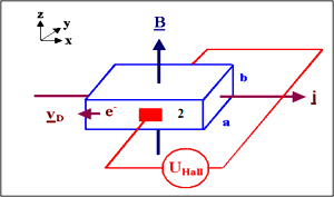
If a specimen carrying a current is placed in transverse magnetic field an electric filed is induced in a direction perpendicular to both electric current and magnetic field. This phenomenon is known as Hall Effect. Let us consider a semiconductor bar of breadth ‘l’ in the in the direction of magnetic field and width ‘d’ carrying a uniform current ‘I’ travelling in X direction and placed in uniform magnetic field ‘B’ in Y direction. Assume the semiconductor current is composed of flow of charge carrier each carrying an electric charge ‘Q’, the Lorentz force on each charge carrier is Fl = Bo*Q*Vo where Vo is velocity of charge carrier and is given by Vo = I/ (l*d*Φ), Φ is charge concentration (or) charge density, the force due to electric field produced by displaced charge is Fe= E*Q. At equilibrium these two forces balances each other
Bo*Q*Vo = E*Q
Electric field produced by displaced charges is equal to E = VH/d, where VH is hall voltage. Hence VH = (Bo* I)/ (l*Φ), VH = (Bo*I*RH)/ l where RH is hall coefficient given by RH = (1/ Φ).
What are the Applications of Hall Effect?
1. Hall Effect is used in measuring magnetic fields (The hall voltage induced in a material is proportional to magnetic field provided the current, carrier density, breadths are kept constant).
2. It is also used in Hall Effect multipliers which provide output proportional to the product of two signals. If the current is made proportional to one of the inputs and if B is linearly related to the second signal, then induced Hall voltage is proportional to the two inputs.
Why hole mobility is less compared to electron?
ANS: Mobility of charge carrier is inversely proportional to the mass of charge carrier. As the hole is having higher effective mass compared to electron for this reason hole mobility is less compared to electron mobility.
Relation between intrinsic carrier concentration with temperature and band gap?
Intrinsic concentration in a semiconductor is given by
Where ni is intrinsic concentration, A is a constant independent of temperature, T is absolute temperature in Kelvin, Ego is band gap at zero degree Kelvin, K is Boltzmann constant.
What is mass action law?
Mass action law states that at equilibrium temperature the product of concentrations of free holes and electrons is equal to the square of intrinsic concentration at that temperature.
No*Po = Ni²,
where No is concentration of electrons in doped semiconductor’s conduction band, Po is concentration of holes in valence band, Ni is intrinsic carrier concentration.
Explain Electrical neutrality based on law of conservation of charge?
Law of conservation of charge states that electric charge can be neither created nor destroyed, total charge is always conserved. Accordingly in an N-type semiconductor the free electron density will increase due to excess charge carriers donated to the conduction band by dopant. After donating the excess electron the dopant atoms will be positively charged (similarly after accepting an electron from valence band acceptor impurity will be negatively charged). Obviously the positive charge of dopant atom exactly balances the excess electron charge by donor which is negative. This is termed as electric neutrality.
What are the types of photo excitation?
There can be two types of photo excitations they are a) intrinsic excitations b) Extrinsic excitations
Intrinsic excitations occur when an electron in valence band is excited by a high energy photon to conduction band. Alternatively a photon may excite an electron in donor level to conduction band or a valence band electron may go into acceptor state. Such excitations are termed as extrinsic excitations.
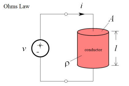
What is ohms law?
ANS: Ohm’s law states that in a conductor current density is directly proportional to applied electric field i.e J α E where J is the current defined as ratio of current to the cross section area trough which the current is flowing and E is the electric field applied. The constant of proportionality is called conductance.
Hence ohm’s law is defined as J = σ*E.
What is Fermi Dirac function?
Fermi Dirac function gives the probability that a energy level with energy ‘E’ will be occupied by an electron. It is given by
Where K is Boltzmann constant, E is the energy of a state in electron volts, Ef is Fermi level, and T is absolute temperature in Kelvin.
What is Fermi level?
Fermi level is the maximum energy that any electron may possess at absolute zero (or) it represents the energy state with 50 percent probability of being filled if no forbidden band exists. The last statements can be explained as follows, at T = 0 K if E > Ef then (E- Ef)/ (KT) tends to positive infinity tends to 0 or maximum energy that any electron may possess at absolute zero then (E- Ef) / (KT) tends to negative infinity tends to 1. Hence the maximum energy that any electron may possess at absolute zero is Fermi level.
Now assume some arbitrary temperature T above 0 Kelvin E = Ef then = (1/2), 50 percent probability of getting filled if no forbidden gap exists.
Equations of conductivity in metal and semiconductors?
Metals conducts current by means of electrons, whereas semiconductors conducts current by two charge carrying particles of opposite sign one is electron(negative charge) and other is hole (positive charge).Therefore the equations for conductivity in metals and semiconductors are
In metals
In semiconductors
Where n is electron concentration, p is hole concentration, Q is electronic charge = 1.6*10^(-19), µn is electron mobility, µp is hole mobility.
What is drift velocity?
In a metal when a voltage is applied between its ends the electrons are accelerated by the voltage applied, while accelerating the electrons experience inelastic collisions with the ions. At each collision electron loses energy and a steady state condition is reached where a finite speed is attained which is known as drift velocity.
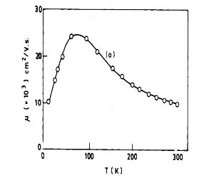
What is the Variation of mobility with temperature?
ANS: As temperature increases at first mobility increases as T^1.5. At these range of temperatures impurity scattering dominates over lattice scattering. It reaches a maximum then mobility starts to decrease as T^-1.5 when lattice scattering dominates impurity scattering.
ANS: In direct band gap semiconductors the highest energy level in valence band and the lowest energy level in conduction band occur at the same momentum or wave number. After the Direct recombination of electron with hole in valence band, energy of the photon released will be exactly equal to difference in energy of lowest energy level in conduction band and highest energy level in valence band.
Note: Momentum and direction of electrons will remain same.
In direct band gap semiconductors the highest energy level in valence band and the lowest energy level in conduction band do not occur at the same momentum or wave number. Since momentum has to be conserved a phonon which is a quantum of vibration energy should exist to assist recombination, hence such recombination of electron with hole are termed as indirect recombination. After the indirect recombination of electron with hole in valence band, energy of the photon released will be less (or) high compared to difference in energy of lowest energy level in conduction band and highest energy level in valence band. This is because some of energy is gained from phonon (or) lost to phonon in recombination process.
Note: Momentum and direction of electron changes after recombination.
Direct and Indirect band gap semiconductor
What is the Variation of mobility with electric field?
At smaller electric fields mobility is constant. At higher electric fields mobility varies inversely with the electric field. At such higher fields the velocity of charge carriers will be constant and is of the order of 2*10^5 m/s. There exists a transition period between these two phases where mobility varies inversely to the square root of electric field.
Intrinsic band diagram extrinsic band diagrams?
Intrinsic semiconductor band diagram
Band diagrams of N-type semiconductor
Band diagrams of P-type semiconductor
Comparison of silicon vs. germanium?
Why silicon is preferred over germanium in electronic devices?
Silicon is preferred over germanium for the following reasons:
- Silicon is abundant in nature is available cheaply.
- The electrical properties of germanium are more sensitive to temperature than silicon. Fine control of conduction properties of germanium is difficult compared to silicon
- Silicon has wider band gap than germanium.
- Silicon is Stable and strong material.
How bands occur in semiconductor?
In a crystal it is found out that the electronic energy levels of atoms gets altered. At interatomic distances the inner shell electros will not be affected much but the outer most energy levels are changed considerably. The outermost shells of all the atoms gets spreads out and forms a large number of discret but closely spaced energy levels called energy bands. In silicon energy band splits into two one is valence band and the other is conduction band.
How can you experimentally differentiate P –type SC and N-type Semi conductor?
If the semiconductor material is of N-type then the carriers will be electrons which are forced towards side 2 by the Lorentz force exerted by the magnetic filed B. Hence the induced hall voltage of side 2 measured with respect to 1(the opposite face to 2) will be negative (Recall that the electrons are negative charge carriers).
If the semiconductor material is of P-type then the carriers will be holes which are forced towards side 2 by the Lorentz force exerted by the magnetic filed B (assuming the flow of current is in the same direction as electrons, conventional current is in the direction opposite to the flow of electrons). Hence the induced hall voltage of side21 measured with respect to 1 (the opposite face to 2) will be positive (Recall that the holes are positive charge carriers).
What is photo electric effect?
When light falls on metal electrons are emitted from the surface of the metal. This phenomena is termed as photo electric effect. The energy the impinging photons (light consists of tiny mass less particles called photons which carry energy of h*v where h is Planck’s constant and v is frequency of light) should be at least equal to work function (characteristic property of metal). If the impinging photon on metal is having energy greater than the work function of metal the extra energy will appear as kinetic energy of ejected electron. Accordingly we can write
h*v = Wf + K.E
Where Wf is the work function of metal, K.E is the kinetic energy of ejected electron.
What is florescence?
Certain substances after absorbing some form of incident electromagnetic radiation releases the absorbed energy in chunks. The emitted radiation will be having lesser energy or frequency compared to the incident radiation. This is termed Fluorescence.
What is the motion of charge particle in electric and magnetic field?
In electrostatic field alone electron moves in straight line. The electron’s travel is in the direction opposite to the direction of electric field.
If an electron enters a magneto static field alone with non zero velocity electron moves in circular path. The electron motion will be in a plane perpendicular to the direction of magnetic field.
If an electron enters a combined electric and magnetic field with non zero velocity electron travels in a helical path whose patch vary with time.
Motion of electron in combined Electric and Magnetic fields
What is thermistor and sensistor?
In semiconductors as temperature increases conductivity increases i.e. it can exhibit positive temperature coefficient of conductivity, this property finds applications in control devices, as a thermal relay e.t.c. Such a semiconductor is called as thermistor.
Sensistor is a heavily doped semiconductor which exhibits positive temperature coefficient of resistance.
What is photo ionization?
When light falls on an atom it will eject one or more electrons (depending on energy of photons) from it forming ions. This process is called Photo ionization. Photo ionization and photo electric effects are one and same process which essentially involves interaction of matter with electromagnetic radiation. The term Photo ionization is used with regard to isolated or non interacting atoms whereas photo electric effect is used with regard to metals.

