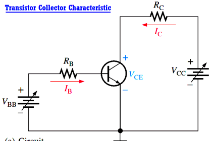
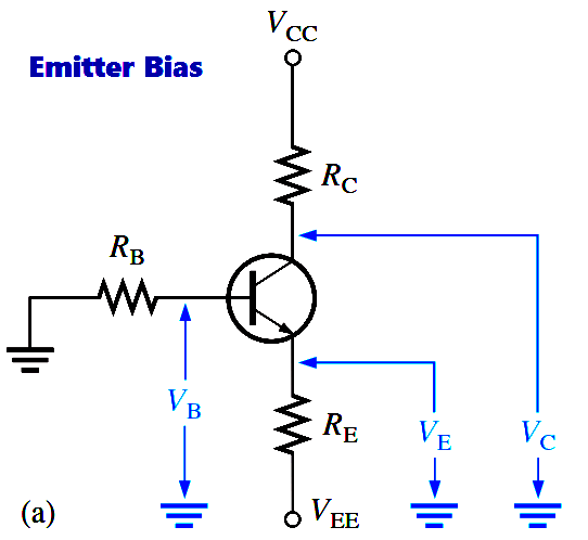
Emitter bias provides excellent bias stability in spite of changes in β or temperature. It uses both a positive and a negative supply voltage. To obtain a reasonable estimate of the key dc values in an emitter-biased circuit, analysis is quite easy. In an npn circuit, such as shown in Figure, the small base current causes the base voltage to be slightly below ground.
The emitter voltage is one diode drop less than this. The combination of this small drop across RB and VBE forces the emitter to be at approximately -1v. Using this approximation, you can obtain the emitter current as
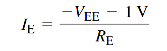
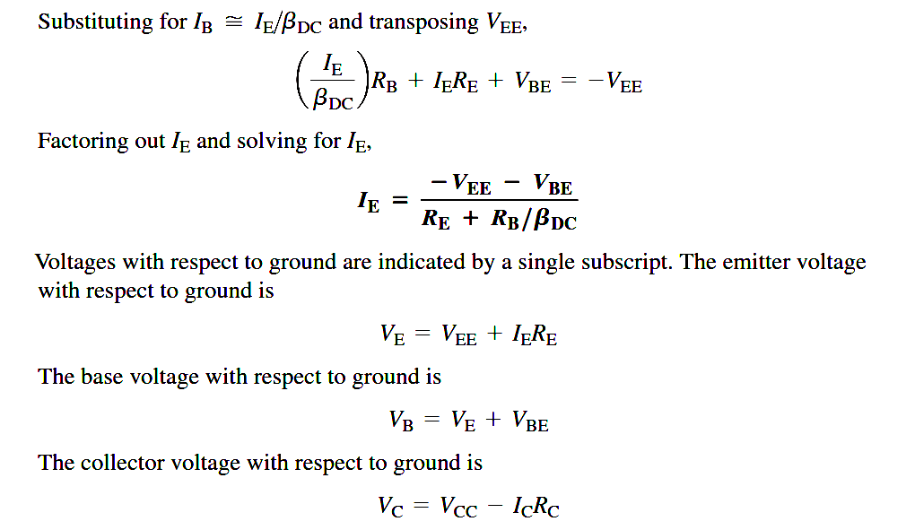
VEE is entered as a negative value in this equation.
You can apply the approximation that IC = IE to calculate the collector voltage.
VC = VCC – ICRC
The approximation that VE = -1v is useful for troubleshooting because you won’t need to perform any detailed calculations. As in the case of voltage-divider bias, there is a more rigorous calculation for cases where you need a more exact result.
The approximation that VE = -1v and the neglect of βDC may not be accurate enough for design work or detailed analysis. In this case, Kirchhoff’s voltage law can be applied as follows to develop a more detailed formula for IE. Kirchhoff’s voltage law applied around the base-emitter circuit in Figure (a), which has been redrawn in part (b) for analysis, gives the following equation:
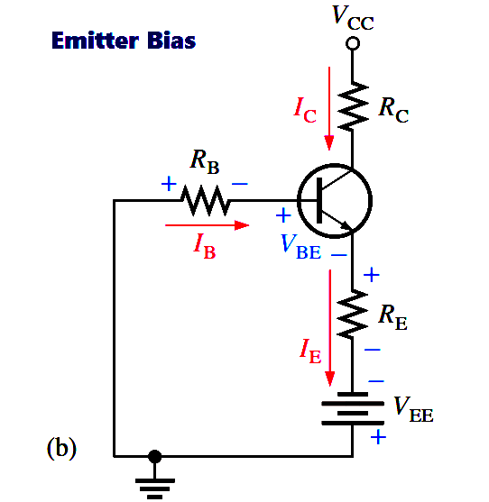
VEE + VRB + VBE + VRE = 0
Substituting, using Ohm’s law,
VEE + IBRB + VBE + IERE = 0