Inst ToolsInst ToolsInst Tools
  • Courses
  • Automation
    • PLC
    • Control System
    • Safety System
    • Communication
    • Fire & Gas System
  • Instrumentation
    • Design
    • Pressure
    • Temperature
    • Flow
    • Level
    • Vibration
    • Analyzer
    • Control Valve
    • Switch
    • Calibration
    • Erection & Commissioning
  • Interview
    • Instrumentation
    • Electrical
    • Electronics
    • Practical
  • Q&A
    • Instrumentation
    • Control System
    • Electrical
    • Electronics
    • Analog Electronics
    • Digital Electronics
    • Power Electronics
    • Microprocessor
  • Request
Search
  • Books
  • Software
  • Projects
  • Process
  • Tools
  • Basics
  • Formula
  • Power Plant
  • Root Cause Analysis
  • Electrical Basics
  • Animation
  • Standards
  • 4-20 mA Course
  • Siemens PLC Course
Reading: Band Gap for Semiconductor Materials
Share
Notification Show More
Font ResizerAa
Inst ToolsInst Tools
Font ResizerAa
  • Courses
  • Design
  • PLC
  • Interview
  • Control System
Search
  • Courses
  • Automation
    • PLC
    • Control System
    • Safety System
    • Communication
    • Fire & Gas System
  • Instrumentation
    • Design
    • Pressure
    • Temperature
    • Flow
    • Level
    • Vibration
    • Analyzer
    • Control Valve
    • Switch
    • Calibration
    • Erection & Commissioning
  • Interview
    • Instrumentation
    • Electrical
    • Electronics
    • Practical
  • Q&A
    • Instrumentation
    • Control System
    • Electrical
    • Electronics
    • Analog Electronics
    • Digital Electronics
    • Power Electronics
    • Microprocessor
  • Request
Follow US
All rights reserved. Reproduction in whole or in part without written permission is prohibited.
Inst Tools > Blog > Electronic Devices & Circuits > Band Gap for Semiconductor Materials

Band Gap for Semiconductor Materials

Last updated: October 5, 2016 1:28 pm
Editorial Staff
Electronic Devices & Circuits
No Comments
Share
2 Min Read
SHARE

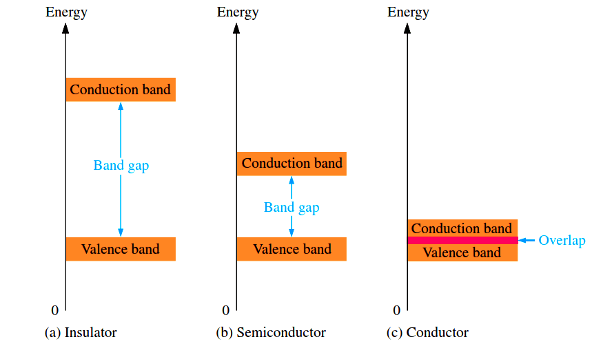
The valence shell of an atom represents a band of energy levels and that the valence electrons are confined to that band. When an electron acquires enough additional energy, it can leave the valence shell, become a free electron, and exist in what is known as the conduction band.

The difference in energy between the valence band and the conduction band is called an energy gap or band gap. This is the amount of energy that a valence electron must have in order to jump from the valence band to the conduction band. Once in the conduction band, the electron is free to move throughout the material and is not tied to any given atom.

The below figure shows energy diagrams for insulators, semiconductors, and conductors. The energy gap or band gap is the difference between two energy levels and is “not allowed” in quantum theory. It is a region in insulators and semiconductors where no electron states exist. Although an electron may not exist in this region, it can “jump” across it under certain conditions. For insulators, the gap can be crossed only when breakdown conditions occur—as when a very high voltage is applied across the material.

The band gap is illustrated in Figure 1–(a) for insulators. In semiconductors the band gap is smaller, allowing an electron in the valence band to jump into the conduction band if it absorbs a photon. The band gap depends on the semiconductor material. This is illustrated in Figure 1–(b). In conductors, the conduction band and valence band overlap, so there is no gap, as shown in Figure 1–(c). This means that electrons in the valence band move freely into the conduction band, so there are always electrons available as free electrons.

energy-diagrams-for-insulator-semiconductor-and-conductor


Don't Miss Our Updates
Be the first to get exclusive content straight to your email.
We promise not to spam you. You can unsubscribe at any time.
Invalid email address
You've successfully subscribed !

Continue Reading

How to Test a Diode using Multimeter
Types of Resistors
Transistor as a Switch Working Principle
Transistor Base Bias
Basic DC Power Supply Circuit
Light Emitting Diode Operation
Share This Article
Facebook Whatsapp Whatsapp LinkedIn Copy Link
Share
Leave a Comment

Leave a Reply Cancel reply

Your email address will not be published. Required fields are marked *

Stay Connected

128.3kFollowersLike
69.1kFollowersFollow
210kSubscribersSubscribe
38kFollowersFollow

Categories

Explore More

Semiconductors Diodes Questions & Answers
Full Wave Bridge Rectifier Peak Inverse Voltage
Short Circuit and Open Circuit
Circuit Elements and Types of Circuits
Optoisolator Working Principle
Bridge Rectifier Working Animation
N Type and P Type Semiconductors
Dependent Current Source

Keep Learning

Types-of-diodes

Different Types of Diodes

seven-segment-display-circuit

Seven Segment Display Working Principle

parallel-resistors-circuit-example

Series and Parallel Resistors

Ideal Diode Characteristics

Ideal Diode Characteristics

MOSFET VI Characteristics

Power MOSFET

diode-limiter-principle

Diode Limiters/Clippers Operation

Comparison of Half wave Rectifiers and Full wave Rectifiers

Comparison of Half wave Rectifiers and Full wave Rectifiers

Transistor Amplifier Working Principle

Learn More

Single Position Calibration of Temperature Bath

Single Position Calibration of Temperature Bath

Fiber Optics Objective Questions and Answers

Fiber Optics Objective Questions and Answers

Bathtub curve

Bathtub Curve

Calibration MCQ - Terminology and Glossary Questions

Calibration MCQ – Terminology and Glossary Questions

Electric Circuits Objective Questions

Electric Circuits Objective Questions – Set 11

Catalytic Gas Sensor Working

Catalytic Type Gas Sensor Principle

Pneumatic Transmitter

Pneumatic Level Transmitter Calibration Table

How to Link SQL With Indusoft Web Studio

How to Use an SQL Server with Indusoft Web Studio?

Menu

  • About
  • Privacy Policy
  • Copyright

Quick Links

  • Learn PLC
  • Helping Hand
  • Part Time Job

YouTube Subscribe

Follow US
All rights reserved. Reproduction in whole or in part without written permission is prohibited.
Welcome Back!

Sign in to your account

Username or Email Address
Password

Lost your password?