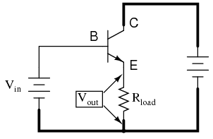
Our next transistor configuration to study is a bit simpler for gain calculations. Called the common-collector configuration, its schematic diagram is shown in Figure below.
common-collector configuration
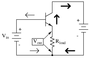
Common collector amplifier has collector common to both input and output.
It is called the common-collector configuration because (ignoring the power supply battery) both the signal source and the load share the collector lead as a common connection point as in Figure below.
Common collector: Input is applied to base and collector. Output is from emitter-collector circuit.
It should be apparent that the load resistor in the common-collector amplifier circuit receives both the base and collector currents, being placed in series with the emitter.
Since the emitter lead of a transistor is the one handling the most current (the sum of base and collector currents, since base and collector currents always mesh together to form the emitter current), it would be reasonable to presume that this amplifier will have a very large current gain.
This presumption is indeed correct: the current gain for a common-collector amplifier is quite large, larger than any other transistor amplifier configuration. However, this is not necessarily what sets it apart from other amplifier designs.
SPICE Analysis
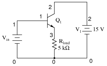
Let\’s proceed immediately to a SPICE analysis of this amplifier circuit, and you will be able to immediately see what is unique about this amplifier. The circuit is in Figure below.
The netlist is in Figure below.
Common collector amplifier for SPICE.
 |
common-collector amplifier vin 1 0 q1 2 1 3 mod1 v1 2 0 dc 15 rload 3 0 5k .model mod1 npn .dc vin 0 5 0.2 .plot dc v(3,0) .end |
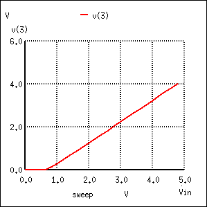
Common collector: Output equals input less a 0.7 V VBE drop.
Unlike the common-emitter amplifier from the previous section, the common-collector produces an output voltage in direct rather than inverse proportion to the rising input voltage.
See Figure above. As the input voltage increases, so does the output voltage. Moreover, a close examination reveals that the output voltage is nearly identical to the input voltage, lagging behind by about 0.7 volts.
This is the unique quality of the common-collector amplifier: an output voltage that is nearly equal to the input voltage.
Examined from the perspective of output voltage change for a given amount of input voltage change, this amplifier has a voltage gain of almost exactly unity (1), or 0 dB. This holds true for transistors of any β value, and for load resistors of any resistance value.
Diode Current Source Transistor Model
It is simple to understand why the output voltage of a common-collector amplifier is always nearly equal to the input voltage.
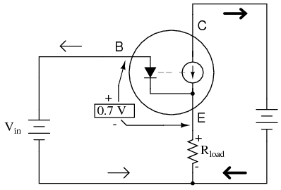
Referring to the diode current source transistor model in Figure below, we see that the base current must go through the base-emitter PN junction, which is equivalent to a normal rectifying diode.
If this junction is forward-biased (the transistor conducting current in either its active or saturated modes), it will have a voltage drop of approximately 0.7 volts, assuming silicon construction.
This 0.7 volt drop is largely irrespective of the actual magnitude of base current; thus, we can regard it as being constant:
Emitter follower: Emitter voltage follows base voltage (less a 0.7 V VBE drop.)
Given the voltage polarities across the base-emitter PN junction and the load resistor, we see that these must add together to equal the input voltage, in accordance with Kirchhoff’s Voltage Law.
In other words, the load voltage will always be about 0.7 volts less than the input voltage for all conditions where the transistor is conducting. Cutoff occurs at input voltages below 0.7 volts, and saturation at input voltages in excess of battery (supply) voltage plus 0.7 volts.
Because of this behavior, the common-collector amplifier circuit is also known as the voltage-follower or emitter-follower amplifier, because the emitter load voltages follow the input so closely.
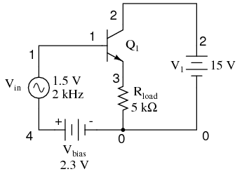
Applying the common-collector circuit to the amplification of AC signals requires the same input “biasing” used in the common-emitter circuit: a DC voltage must be added to the AC input signal to keep the transistor in its active mode during the entire cycle. When this is done, the result is the non-inverting amplifier in Figure below.
 |
common-collector amplifier vin 1 4 sin(0 1.5 2000 0 0) vbias 4 0 dc 2.3 q1 2 1 3 mod1 v1 2 0 dc 15 rload 3 0 5k .model mod1 npn .tran .02m .78m .plot tran v(1,0) v(3,0) .end |
Common collector (emitter-follower) amplifier.
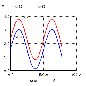
The results of the SPICE simulation in Figure below show that the output follows the input. The output is the same peak-to-peak amplitude as the input. Though, the DC level is shifted downward by one VBE diode drop.
Common collector (emitter-follower): Output V3 follows input V1 less a 0.7 V VBE drop.
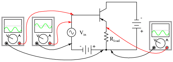
Here\’s another view of the circuit (Figure below) with oscilloscopes connected to several points of interest.
Common collector non-inverting voltage gain is 1.
Since this amplifier configuration doesn\’t provide any voltage gain (in fact, in practice it actually has a voltage gain of slightly less than 1), its only amplifying factor is current.
The common-emitter amplifier configuration examined in the previous section had a current gain equal to the β of the transistor, being that the input current went through the base and the output (load) current went through the collector, and β by definition is the ratio between the collector and base currents.
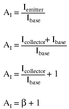
In the common-collector configuration, though, the load is situated in series with the emitter, and thus its current is equal to the emitter current. With the emitter carrying collector current and base current, the load in this type of amplifier has all the current of the collector running through it plus the input current of the base. This yields a current gain of β plus 1:
Once again, PNP transistors are just as valid to use in the common-collector configuration as NPN transistors. The gain calculations are all the same, as is the non-inverting of the amplified signal.
The only difference is in voltage polarities and current directions shown in Figure below.
PNP version of the common-collector amplifier.
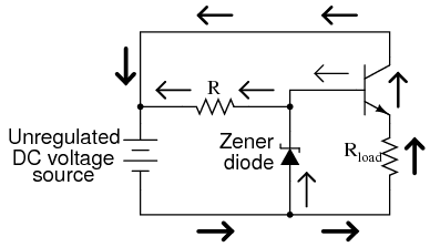
A popular application of the common-collector amplifier is for regulated DC power supplies, where an unregulated (varying) source of DC voltage is clipped at a specified level to supply regulated (steady) voltage to a load.
Zener diode voltage regulator
Of course, zener diodes already provide this function of voltage regulation shown in Figure below.
Zener diode voltage regulator.
However, when used in this direct fashion, the amount of current that may be supplied to the load is usually quite limited.
In essence, this circuit regulates voltage across the load by keeping current through the series resistor at a high enough level to drop all the excess power source voltage across it, the zener diode drawing more or less current as necessary to keep the voltage across itself steady.
For high-current loads, a plain zener diode voltage regulator would have to shunt a heavy current through the diode to be effective at regulating load voltage in the event of large load resistance or voltage source changes.
One popular way to increase the current-handling ability of a regulator circuit like this is to use a common-collector transistor to amplify current to the load, so that the zener diode circuit only has to handle the amount of current necessary to drive the base of the transistor. (Figure below)
Common collector application: voltage regulator.
There\’s really only one caveat to this approach: the load voltage will be approximately 0.7 volts less than the zener diode voltage, due to the transistor\’s 0.7 volt base-emitter drop.
Since this 0.7 volt difference is fairly constant over a wide range of load currents, a zener diode with a 0.7 volt higher rating can be chosen for the application.
Darlington pair
Sometimes the high current gain of a single-transistor, common-collector configuration isn\’t enough for a particular application.
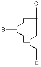
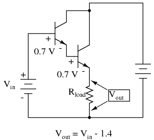
If this is the case, multiple transistors may be staged together in a popular configuration known as a Darlington pair, just an extension of the common-collector concept shown in Figure below.
An NPN darlington pair.
Darlington pairs essentially place one transistor as the common-collector load for another transistor, thus multiplying their individual current gains.
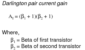
Base current through the upper-left transistor is amplified through that transistor\’s emitter, which is directly connected to the base of the lower-right transistor, where the current is again amplified. The overall current gain is as follows:
Voltage gain is still nearly equal to 1 if the entire assembly is connected to a load in common-collector fashion, although the load voltage will be a full 1.4 volts less than the input voltage shown in Figure below.
Darlington pair based common-collector amplifier loses two VBE diode drops.
Darlington pairs may be purchased as discrete units (two transistors in the same package), or may be built up from a pair of individual transistors. Of course, if even more current gain is desired than what may be obtained with a pair, Darlington triplet or quadruplet assemblies may be constructed.
Review
Common-collector transistor amplifiers are so-called because the input and output voltage points share the collector lead of the transistor in common with each other, not considering any power supplies.
The common-collector amplifier is also known as an emitter-follower.
The output voltage on a common-collector amplifier will be in phase with the input voltage, making the common-collector a non-inverting amplifier circuit.
The current gain of a common-collector amplifier is equal to β plus 1. The voltage gain is approximately equal to 1 (in practice, just a little bit less).
A Darlington pair is a pair of transistors “piggybacked” on one another so that the emitter of one feeds current to the base of the other in common-collector form. The result is an overall current gain equal to the product (multiplication) of their individual common-collector current gains (β plus 1).
