The SPICE circuit simulation program provides for modeling diodes in circuit simulations.
The diode model is based on characterization of individual devices as described in a product data sheet and manufacturing process characteristics not listed.
Some information has been extracted from a 1N4004 data sheet in Figure below.
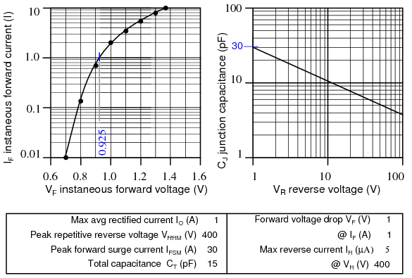
Data sheet 1N4004 excerpt, after [DI4].
The diode statement begins with a diode element name which must begin with “d” plus optional characters. Example diode element names include: d1, d2, dtest, da, db, d101.
Two node numbers specify the connection of the anode and cathode, respectively, to other components. The node numbers are followed by a model name, referring to a subsequent “.model” statement.
The model statement line begins with “.model,” followed by the model name matching one or more diode statements. Next, a “d” indicates a diode is being modeled.
The remainder of the model statement is a list of optional diode parameters of the form ParameterName=ParameterValue. None are used in Example below.
Example2 has some parameters defined.
For a list of diode parameters, see Table below.
 General form:  d[name] [anode] [cathode] [modelname]
                .model ([modelname] d [parmtr1=x] [parmtr2=y] . . .)

 Example:       d1 1 2 mod1
                 .model mod1 d

 Example2:      D2 1 2 Da1N4004
               .model Da1N4004 D (IS=18.8n RS=0 BV=400 IBV=5.00u CJO=30 M=0.333 N=2)
The easiest approach to take for a SPICE model is the same as for a data sheet: consult the manufacturer\’s web site. Table below lists the model parameters for some selected diodes. A fallback strategy is to build a SPICE model from those parameters listed on the data sheet.
A third strategy, not considered here, is to take measurements of an actual device. Then, calculate, compare and adjust the SPICE parameters to the measurements.
Diode SPICE parameters
| Symbol | Name | Parameter | Units | Default |
|---|---|---|---|---|
| IS | IS | Saturation current (diode equation) | A | 1E-14 |
| RS | RS | Parsitic resistance (series resistance) | Ω | 0 |
| n | N | Emission coefficient, 1 to 2 | – | 1 |
| τD | TT | Transit time | s | 0 |
| CD(0) | CJO | Zero-bias junction capacitance | F | 0 |
| φ0 | VJ | Junction potential | V | 1 |
| m | M | Junction grading coefficient | – | 0.5 |
| – | – | 0.33 for linearly graded junction | – | – |
| – | – | 0.5 for abrupt junction | – | – |
| Eg | EG | Activation energy: | eV | 1.11 |
| – | – | Si: 1.11 | – | – |
| – | – | Ge: 0.67 | – | – |
| – | – | Schottky: 0.69 | – | – |
| pi | XTI | IS temperature exponent | – | 3.0 |
| – | – | pn junction: 3.0 | – | – |
| – | – | Schottky: 2.0 | – | – |
| kf | KF | Flicker noise coefficient | – | 0 |
| af | AF | Flicker noise exponent | – | 1 |
| FC | FC | Forward bias depletion capacitance coefficient | – | 0.5 |
| BV | BV | Reverse breakdown voltage | V | ∞ |
| IBV | IBV | Reverse breakdown current | A | 1E-3 |
If diode parameters are not specified as in “Example” model above, the parameters take on the default values listed in Table above and Table below. These defaults model integrated circuit diodes. These are certainly adequate for preliminary work with discrete devices
For more critical work, use SPICE models supplied by the manufacturer [DIn], SPICE vendors, and other sources.
SPICE parameters
for selected diodes; sk=schottky Ge=germanium; else silicon.
| Part | IS | RS | N | TT | CJO | M | VJ | EG | XTI | BV | IBV |
|---|---|---|---|---|---|---|---|---|---|---|---|
| Default | 1E-14 | 0 | 1 | 0 | 0 | 0.5 | 1 | 1.11 | 3 | ∞ | 1m |
| 1N5711 sk | 315n | 2.8 | 2.03 | 1.44n | 2.00p | 0.333 | – | 0.69 | 2 | 70 | 10u |
| 1N5712 sk | 680p | 12 | 1.003 | 50p | 1.0p | 0.5 | 0.6 | 0.69 | 2 | 20 | – |
| 1N34 Ge | 200p | 84m | 2.19 | 144n | 4.82p | 0.333 | 0.75 | 0.67 | – | 60 | 15u |
| 1N4148 | 35p | 64m | 1.24 | 5.0n | 4.0p | 0.285 | 0.6 | – | – | 75 | – |
| 1N3891 | 63n | 9.6m | 2 | 110n | 114p | 0.255 | 0.6 | – | – | 250 | – |
| 10A04 10A | 844n | 2.06m | 2.06 | 4.32u | 277p | 0.333 | – | – | – | 400 | 10u |
| 1N4004 1A | 76.9n | 42.2m | 1.45 | 4.32u | 39.8p | 0.333 | – | – | – | 400 | 5u |
| 1N4004 data sheet | 18.8n | – | 2 | – | 30p | 0.333 | – | – | – | 400 | 5u |
Otherwise, derive some of the parameters from the data sheet. First select a value for spice parameter N between 1 and 2. It is required for the diode equation (n). Massobrio pp 9, recommends “.. n, the emission coefficient is usually about 2.”
In Table above, we see that power rectifiers 1N3891 (12 A), and 10A04 (10 A) both use about 2. The first four in the table are not relevant because they are schottky, schottky, germanium, and silicon small signal, respectively.
The saturation current, IS, is derived from the diode equation, a value of (VD, ID) on the graph in Figure above, and N=2 (n in the diode equation).
      ID =  IS(eVD/nVT -1)

      VT = 26 mV at 25oC       n = 2.0    VD = 0.925 V at 1 A from graph

      1 A =  IS(e(0.925 V)/(2)(26 mV) -1)

      IS =  18.8E-9
The numerical values of IS=18.8n and N=2 are entered in last line of Table above for comparison to the manufacturers model for 1N4004, which is considerably different. RS defaults to 0 for now. It will be estimated later. The important DC static parameters are N, IS, and RS.
Rashid suggests that TT, τD, the transit time, be approximated from the reverse recovery stored charge QRR, a data sheet parameter (not available on our data sheet) and IF, forward current.
      ID =  IS(eVD/nVT -1)

      τD =  QRR/IF
We take the TT=0 default for lack of QRR. Though it would be reasonable to take TT for a similar rectifier like the 10A04 at 4.32u. The 1N3891 TT is not a valid choice because it is a fast recovery rectifier. CJO, the zero bias junction capacitance is estimated from the VR vs CJ graph in Figure above.
The capacitance at the nearest to zero voltage on the graph is 30 pF at 1 V. If simulating high speed transient response, as in switching regulator power supplies, TT and CJO parameters must be provided.
The junction grading coefficient M is related to the doping profile of the junction. This is not a data sheet item. The default is 0.5 for an abrupt junction. We opt for M=0.333 corresponding to a linearly graded junction. The power rectifiers in Table above use lower values for M than 0.5.
We take the default values for VJ and EG. Many more diodes use VJ=0.6 than shown in Table above. However the 10A04 rectifier uses the default, which we use for our 1N4004 model (Da1N4001 in Table above). Use the default EG=1.11 for silicon diodes and rectifiers.
Table above lists values for schottky and germanium diodes. Take the XTI=3, the default IS temperature coefficient for silicon devices. See Table above for XTI for schottky diodes.
The abbreviated data sheet, Figure above, lists IR = 5 µA @ VR = 400 V, corresponding to IBV=5u and BV=400 respectively. The 1n4004 SPICE parameters derived from the data sheet are listed in the last line of Table above for comparison to the manufacturer\’s model listed above it.
BV is only necessary if the simulation exceeds the reverse breakdown voltage of the diode, as is the case for zener diodes. IBV, reverse breakdown current, is frequently omitted, but may be entered if provided with BV.
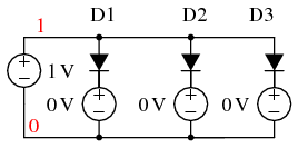
Figure below shows a circuit to compare the manufacturers model, the model derived from the datasheet, and the default model using default parameters. The three dummy 0 V sources are necessary for diode current measurement.
The 1 V source is swept from 0 to 1.4 V in 0.2 mV steps. See .DC statement in the netlist in Table below. DI1N4004 is the manufacturer\’s diode model, Da1N4004 is our derived diode model.
SPICE circuit for comparison of manufacturer model (D1), calculated datasheet model (D2), and default model (D3).
SPICE netlist parameters: (D1) DI1N4004 manufacturer\’s model, (D2) Da1N40004 datasheet derived, (D3) default diode model.
*SPICE circuit <03468.eps> from XCircuit v3.20
D1 1 5 DI1N4004
V1 5 0 0
D2 1 3 Da1N4004
V2 3 0 0
D3 1 4 Default
V3 4 0 0
V4 1 0 1
.DC V4 0 1400mV 0.2m
.model Da1N4004 D (IS=18.8n RS=0      BV=400 IBV=5.00u CJO=30
 M=0.333   N=2.0  TT=0)
.MODEL DI1N4004 D (IS=76.9n RS=42.0m  BV=400 IBV=5.00u CJO=39.8p
 M=0.333 N=1.45 TT=4.32u)
.MODEL Default D
.end
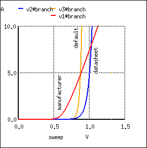
We compare the three models in Figure below. and to the datasheet graph data in Table below. VD is the diode voltage versus the diode currents for the manufacturer\’s model, our calculated datasheet model and the default diode model.
The last column “1N4004 graph” is from the datasheet voltage versus current curve in Figure above which we attempt to match.
Comparison of the currents for the three model to the last column shows that the default model is good at low currents, the manufacturer\’s model is good at high currents, and our calculated datasheet model is best of all up to 1 A.
Agreement is almost perfect at 1 A because the IS calculation is based on diode voltage at 1 A. Our model grossly over states current above 1 A.
First trial of manufacturer model, calculated datasheet model, and default model.
Comparison of manufacturer model, calculated datasheet model, and default model to 1N4004 datasheet graph of V vs I.
                        model            model           model         1N4004
index      VD           manufacturer     datasheet       default        graph
3500    7.000000e-01    1.612924e 00    1.416211e-02    5.674683e-03    0.01
4001    8.002000e-01    3.346832e 00    9.825960e-02    2.731709e-01    0.13
4500    9.000000e-01    5.310740e 00    6.764928e-01    1.294824e 01    0.7
4625    9.250000e-01    5.823654e 00    1.096870e 00    3.404037e 01    1.0
5000    1.000000e-00    7.395953e 00    4.675526e 00    6.185078e 02    2.0
5500    1.100000e 00    9.548779e 00    3.231452e 01    2.954471e 04    3.3
6000    1.200000e 00    1.174489e 01    2.233392e 02    1.411283e 06    5.3
6500    1.300000e 00    1.397087e 01    1.543591e 03    6.741379e 07    8.0
7000    1.400000e 00    1.621861e 01    1.066840e 04    3.220203e 09   12.
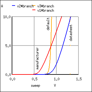
The solution is to increase RS from the default RS=0. Changing RS from 0 to 8m in the datasheet model causes the curve to intersect 10 A (not shown) at the same voltage as the manufacturer\’s model. Increasing RS to 28.6m shifts the curve further to the right as shown in Figure below.
This has the effect of more closely matching our datasheet model to the datasheet graph (Figure above). Table below shows that the current 1.224470e 01 A at 1.4 V matches the graph at 12 A. However, the current at 0.925 V has degraded from 1.096870e 00 above to 7.318536e-01.
Second trial to improve calculated datasheet model compared with manufacturer model and default model.
Changing Da1N4004 model statement RS=0 to RS=28.6m decreases the current at VD=1.4 V to 12.2 A.
.model Da1N4004 D (IS=18.8n RS=28.6m  BV=400 IBV=5.00u CJO=30
 M=0.333   N=2.0  TT=0)
                        model            model           1N4001
index      VD           manufacturer     datasheet        graph
3505    7.010000e-01    1.628276e 00    1.432463e-02      0.01
4000    8.000000e-01    3.343072e 00    9.297594e-02      0.13
4500    9.000000e-01    5.310740e 00    5.102139e-01      0.7
4625    9.250000e-01    5.823654e 00    7.318536e-01      1.0
5000    1.000000e-00    7.395953e 00    1.763520e 00      2.0
5500    1.100000e 00    9.548779e 00    3.848553e 00      3.3
6000    1.200000e 00    1.174489e 01    6.419621e 00      5.3
6500    1.300000e 00    1.397087e 01    9.254581e 00      8.0
7000    1.400000e 00    1.621861e 01    1.224470e 01     12.
Suggested reader exercise: decrease N so that the current at VD=0.925 V is restored to 1 A. This may increase the current (12.2 A) at VD=1.4 V requiring an increase of RS to decrease current to 12 A.
Zener diode
There are two approaches to modeling a zener diode: set the BV parameter to the zener voltage in the model statement, or model the zener with a subcircuit containing a diode clamper set to the zener voltage.
An example of the first approach sets the breakdown voltage BV to 15 for the 1n4469 15 V zener diode model (IBV optional):
.model D1N4469 D ( BV=15 IBV=17m )
The second approach models the zener with a subcircuit. Clamper D1 and VZ in Figure below models the 15 V reverse breakdown voltage of a 1N4477A zener diode.
Diode DR accounts for the forward conduction of the zener in the subcircuit.
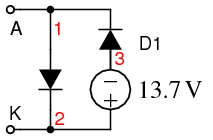 |
.SUBCKT DI-1N4744A 1 2 * Terminals A K D1 1 2 DF DZ 3 1 DR VZ 2 3 13.7 .MODEL DF D ( IS=27.5p RS=0.620 N=1.10 CJO=78.3p VJ=1.00 M=0.330 TT=50.1n ) .MODEL DR D ( IS=5.49f RS=0.804 N=1.77 ) .ENDS |
Zener diode subcircuit uses clamper (D1 and VZ) to model zener.
Tunnel diode: A tunnel diode may be modeled by a pair of field effect transistors (JFET) in a SPICE subcircuit. An oscillator circuit is also shown in this reference.
Gunn diode: A Gunn diode may also be modeled by a pair of JFET\’s. This reference shows a microwave relaxation oscillator.
Review
Diodes are described in SPICE by a diode component statement referring to .model statement. The .model statement contains parameters describing the diode. If parameters are not provided, the model takes on default values.
Static DC parameters include N, IS, and RS. Reverse breakdown parameters: BV, IBV.
Accurate dynamic timing requires TT and CJO parameters
Models provided by the manufacturer are highly recommended.
