Most integrated circuits are digital, based on MOS (CMOS) transistors. Every couple of years since the late 1960\’s a geometry shrink has taken place, increasing the circuit density– more circuitry at lower cost in the same space.
As of this writing (2006), the MOS transistor gate length is 65-nm for leading edge production, with 45-nm anticipated within a year. At 65-nm leakage currents were becoming evident. At 45-nm, heroic innovations were required to minimize this leakage.
The end of shrinkage in MOS transistors is expected at 20- to 30-nm. Though some think that 1- to 2-nm is the limit. Photolithography, or other lithographic techniques, will continue to improve, providing ever smaller geometry. However, conventional MOS transistors are not expected to be usable at these smaller geometries below 20- to 30-nm.
Improved photolithography will have to be applied to other than the conventional transistors, dimensions (under 20- to 30-nm). The objectional MOS leakage currents are due to quantum mechanical effects–electron tunneling through gate oxide, and the narrow channel.
In summary, quantum mechanical effects are a hindrance to ever smaller conventional MOS transistors. The path to ever smaller geometry devices involves unique active devices which make practical use of quantum mechanical principles.
As physical geometry becomes very small, electrons may be treated as the quantum mechanical equivalent: a wave. Devices making use of quantum mechanical principles include: resonant tunneling diodes, quantum tunneling transistors, metal insulator metal diodes, and quantum dot transistors.
Quantum Tunneling
It is the passing of electrons through an insulating barrier which is thin compared to the de Broglie (here) electron wavelength. If the “electron wave” is large compared to the barrier, there is a possibility that the wave appears on both sides of the barrier.
Classical view of an electron surmounting a barrier, or not. Quantum mechanical view allows an electron to tunnel through a barrier. The probability (green) is related to the barrier thickness. After Figure 1
In classical physics, an electron must have sufficient energy to surmount a barrier. Otherwise, it recoils from the barrier. (Figure above) Quantum mechanics allows for a probability of the electron being on the other side of the barrier.
If treated as a wave, the electron may look quite large compared to the thickness of the barrier. Even when treated as a wave, there is only a small probability that it will be found on the other side of a thick barrier. See green portion of curve, Figure above. Thinning the barrier increases the probability that the electron is found on the other side of the barrier.
Tunnel diode
The unqualified term tunnel diode refers to the esaki tunnel diode, an early quantum device. A reverse biased diode forms a depletion region, an insulating region, between the conductive anode and cathode.
This depletion region is only thin as compared to the electron wavelength when heavily doped– 1000 times the doping of a rectifier diode. With proper biasing, quantum tunneling is possible. See CH 3 for details.
RTD, resonant tunneling diode
This is a quantum device not to be confused with the Esaki tunnel diode, CH 3 , a conventional heavily doped bipolar semiconductor. Electrons tunnel through two barriers separated by a well in flowing source to drain in a resonant tunneling diode.
Tunneling is also known as quantum mechanical tunneling. The flow of electrons is controlled by diode bias. This matches the energy levels of the electrons in the source to the quantized level in the well so that electrons can tunnel through the barriers.
The energy level in the well is quantized because the well is small. When the energy levels are equal, a resonance occurs, allowing electron flow through the barriers as shown in Figure below (b).
No bias or too much bias, in Figures below (a) and (c) respectively, yields an energy mismatch between the source and the well, and no conduction.
Resonant tunneling diode (RTD): (a) No bias, source and well energy levels not matched, no conduction. (b) Small bias causes matched energy levels (resonance); conduction results. (c) Further bias mismatches energy levels, decreasing conduction.
As bias is increased from zero across the RTD, the current increases and then decreases, corresponding to off, on, and off states. This makes simplification of conventional transistor circuits possible by substituting a pair of RTD\’s for two transistors.
For example, two back-to-back RTD\’s and a transistor form a memory cell, using fewer components, less area and power compared with a conventional circuit.
The potential application of RTD\’s is to reduce the component count, area, and power dissipation of conventional transistor circuits by replacing some, though not all, transistors. RTD\’s have been shown to oscillate up to 712 gHz.
Double-layer tunneling transistor
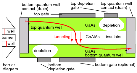
The Deltt, otherwise known as the Double-layer tunneling transistor is constructed of a pair of conductive wells separated by an insulator or high band gap semiconductor. (Figure below) The wells are so thin that electrons are confined to two dimensions. These are known as quantum wells.
A pair of these quantum wells are insulated by a thin GaAlAs, high band gap (does not easily conduct) layer. Electrons can tunnel through the insulating layer if the electrons in the two quantum wells have the same momentum and energy.
The wells are so thin that the electron may be treated as a wave– the quantum mechanical duality of particles and waves. The top and optional bottom control gates may be adjusted to equalize the energy levels (resonance) of the electrons to allow conduction from source to drain.
Figure below, barrier diagram red bars show unequal energy levels in the wells, an “off-state” condition. Proper biasing of the gates equalizes the energy levels of electrons in the wells, the “on-state” condition. The bars would be at the same level in the energy level diagram.
Double-layer tunneling transistor (Deltt) is composed of two electron containing wells separated by a nonconducting barrier. The gate voltages may be adjusted so that the energy and momentum of the electrons in the wells are equal which permits electrons to tunnel through the nonconductive barrier. (The energy levels are shown as unequal in the barrier diagram.)
If gate bias is increased beyond that required for tunneling, the energy levels in the quantum wells no longer match, tunneling is inhibited, source to drain current decreases. To summarize, increasing gate bias from zero results in on, off, on conditions.
This allows a pair of Deltt\’s to be stacked in the manner of a CMOS complementary pair; though, different p- and n-type transistors are not required. Power supply voltage is about 100 mV. Experimental Deltt\’s have been produced which operate near 4.2 K, 77 K, and 0o C. Room temperature versions are expected.
Metal Insulator Insulator Metal Diode
The metal-insulator-insulator-metal (MIIM) diode is a quantum tunneling device, not based on semiconductors. See “MIIM diode section” Figure below.
The insulator layers must be thin compared to the de Broglie (here) electron wavelength, for quantum tunneling to be possible. For diode action, there must be a preferred tunneling direction, resulting in a sharp bend in the diode forward characteristic curve.
The MIIM diode has a sharper forward curve than the metal insulator metal (MIM) diode, not considered here.
Metal insulator insulator metal (MIIM) diode: Cross section of diode. Energy levels for no bias, forward bias, and reverse bias. After Figure 1
The energy levels of M1 and M2 are equal in “no bias” Figure above. However, (thermal) electrons cannot flow due to the high I1 and I2 barriers. Electrons in metal M2 have a higher energy level in “reverse bias” Figure above, but still cannot overcome the insulator barrier.
As “forward bias” Figure above is increased, a quantum well, an area where electrons may exist, is formed between the insulators. Electrons may pass through insulator I1 if M1 is bised at the same energy level as the quantum well.
A simple explanation is that the distance through the insulators is shorter. A longer explanation is that as bias increases, the probability of the electron wave overlapping from M1 to the quantum well increases. For a more detailed explanation see Phiar Corp.
MIIM devices operate at higher frequencies (3.7 THz) than microwave transistors. The addition of a third electrode to a MIIM diode produces a transistor.
Quantum dot transistor
An isolated conductor may take on a charge, measured in coulombs for large objects. For a nano-scale isolated conductor known as a quantum dot, the charge is measured in electrons. A quantum dot of 1- to 3-nm may take on an incremental charge of a single electron. This is the basis of the quantum dot transistor, also known as a single electron transistor.
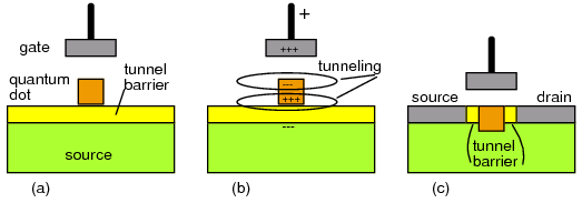
A quantum dot placed atop a thin insulator over an electron rich source is known as a single electron box. (Figure below (a)) The energy required to transfer an electron is related to the size of the dot and the number of electrons already on the dot.
A gate electrode above the quantum dot can adjust the energy level of the dot so that quantum mechanical tunneling of an electron (as a wave) from the source through the insulator is possible. (Figure below (b)) Thus, a single electron may tunnel to the dot.
(a) Single electron box, an isolated quantum dot separated from an electron source by an insulator. (b) Positive charge on the gate polarizes quantum dot, tunneling an electron from the source to the dot. (c) Quantum transistor: channel is replaced by quantum dot surrounded by tunneling barrier.
If the quantum dot is surrounded by a tunnel barrier and embedded between the source and drain of a conventional FET, as in Figure above (c) , the charge on the dot can modulate the flow of electrons from source to drain. As gate voltage increases, the source to drain current increases, up to a point.
A further increase in gate voltage decreases drain current. This is similar to the behavior of the RTD and Deltt resonant devices. Only one kind of transistor is required to build a complementary logic gate.
Single Electron Transistor
If a pair of conductors, superconductors, or semiconductors are separated by a pair of tunnel barriers (insulator), surrounding a tiny conductive island, like a quantum dot, the flow of a single charge (a Cooper pair for superconductors) may be controlled by a gate. This is a single electron transistor similar to Figure above (c).
Increasing the positive charge on the gate, allows an electron to tunnel to the island. If it is sufficiently small, the low capacitance will cause the dot potential to rise substantially due to the single electron. No more electrons can tunnel to the island due the electron charge.
This is known at the coulomb blockade. The electron which tunneled to the island, can tunnel to the drain.
Single electron transistors operate at near absolute zero. The exception is the graphene single electron transistor, having a graphene island. They are all experimental devices.
Graphene Transistor
Graphite, an allotrope of carbon, does not have the rigid interlocking crystalline structure of diamond. None the less, it has a crystalline structure– one atom thick, a so called two-dimensional structure.
A graphite is a three-dimensional crystal. However, it cleaves into thin sheets. Experimenters, taking this to the extreme, produce micron sized specks as thin as a single atom known as graphene. (Figure below (a)) These membranes have unique electronic properties. Highly conductive, conduction is by either electrons or holes, without doping of any kind.
Graphene sheets may be cut into transistor structures by lithographic techniques. The transistors bear some resemblance to a MOSFET. A gate capacitively coupled to a graphene channel controls conduction.
As silicon transistors scale to smaller sizes, leakage increases along with power dissipation. And they get smaller every couple of years. Graphene transistors dissipate little power. And, they switch at high speed. Graphene might be a replacement for silicon someday.
Graphene can be fashioned into devices as small as sixty atoms wide. Graphene quantum dots within a transistor this small serve as single electron transistors. Previous single electron transistors fashioned from either superconductors or conventional semiconductors operate near absolute zero. Graphene single electron transistors uniquely function at room temperature.
Graphene transistors are laboratory curiosities at this time. If they are to go into production two decades from now, graphene wafers must be produced. The first step, production of graphene by chemical vapor deposition (CVD) has been accomplished on an experimental scale. Though, no wafers are available to date.
(a) Graphene: A single sheet of the graphite allotrope of carbon. The atoms are arranged in a hexagonal pattern with a carbon at each intersection. (b) Carbon nanotube: A rolled-up sheet of graphene.
Carbon nanotube transistor
If a 2-D sheet of graphene is rolled, the resulting 1-D structure is known as a carbon nanotube. (Figure above (b)) The reason to treat it as 1-dimensional is that it is highly conductive. Electrons traverse the carbon nanotube without being scattered by a crystal lattice.
Resistance in normal metals is caused by scattering of electrons by the metallic crystalline lattice. If electrons avoid this scattering, conduction is said to be by ballistic transport. Both metallic (acting) and semiconducting carbon nanotubes have been produced.
Field effect transistors may be fashioned from a carbon nanotubes by depositing source and drain contacts on the ends, and capacitively coupling a gate to the nanotube between the contacts.
Both p- and n-type transistors have been fabricated. Why the interest in carbon nanotube transistors? Nanotube semiconductors are Smaller, faster, lower power compared with silicon transistors.
Spintronics
Conventional semiconductors control the flow of electron charge, current. Digital states are represented by “on” or “off” flow of current. As semiconductors become more dense with the move to smaller geometry, the power that must be dissipated as heat increases to the point that it is difficult to remove. Electrons have properties other than charge such as spin.
A tentative explanation of electron spin is the rotation of distributed electron charge about the spin axis, analogous to diurnal rotation of the Earth. The loops of current created by charge movement, form a magnetic field.
However, the electron is more like a point charge than a distributed charge, Thus, the rotating distributed charge analogy is not a correct explanation of spin. Electron spin may have one of two states: up or down which may represent digital states. More precisely the spin (ms) quantum number may be ±1/2 the angular momentum (l) quantum number.
Controlling electron spin instead of charge flow considerably reduces power dissipation and increases switching speed. Spintronics, an acronym for SPIN TRansport electrONICS, is not widely applied because of the difficulty of generating, controlling, and sensing electron spin.
However, high density, non-volatile magnetic spin memory is in production using modified semiconductor processes. This is related to the spin valve magnetic read head used in computer harddisk drives, not mentioned further here.
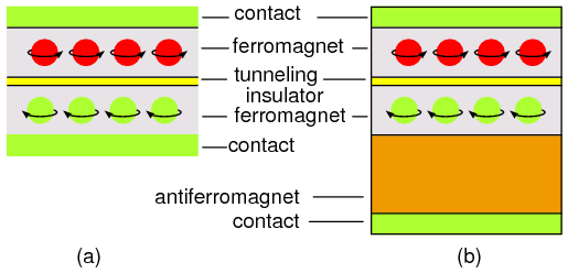
A simple magnetic tunnel junction (MTJ) is shown in Figure below (a), consisting of a pair of ferromagnetic, strong magnetic properties like iron (Fe), layers separated by a thin insulator. Electrons can tunnel through a sufficiently thin insulator due to the quantum mechanical properties of electrons– the wave nature of electrons.
The current flow through the MTJ is a function of the magnetization, spin polarity, of the ferromagnetic layers. The resistance of the MTJ is low if the magnetic spin of the top layer is in the same direction (polarity) as the bottom layer. If the magnetic spins of the two layers oppose, the resistance is higher.
(a) Magnetic tunnel junction (MTJ): Pair of ferromagnetic layers separated by a thin insulator. The resistance varies with the magnetization polarity of the top layer (b) Antiferromagnetic bias magnet and pinned bottom ferromagnetic layer increases resistance sensitivity to changes in polarity of the top ferromagnetic layer. Adapted from Figure 3.
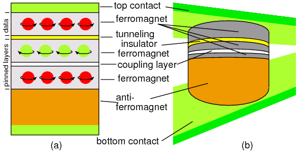
The change in resistance can be enhanced by the addition of an antiferromagnet, material having spins aligned but opposing, below the bottom layer in Figure above (b). This bias magnet pins the lower ferromagnetic layer spin to a single unchanging polarity.
The top layer magnetization (spin) may be flipped to represent data by the application of an external magnetic field not shown in the figure. The pinned layer is not affected by external magnetic fields. Again, the MTJ resistance is lowest when the spin of the top ferromagnetic layer is the same sense as the bottom pinned ferromagnetic layer.
The MTJ may be improved further by splitting the pinned ferromagnetic layer into two layers separated by a buffer layer in Figure below (a). This isolates the top layer. The bottom ferromagnetic layer is pinned by the antiferromagnet as in the previous figure.
The ferromagnetic layer atop the buffer is attracted by the bottom ferromagnetic layer. Opposites attract. Thus, the spin polarity of the additional layer is opposite of that in the bottom layer due to attraction. The bottom and middle ferromagnetic layers remain fixed.
The top ferromagnetic layer may be set to either spin polarity by high currents in proximate conductors (not shown). This is how data are stored. Data are read out by the difference in current flow through the tunnel junction. Resistance is lowest if the layers on both sides of the insulating layer are of the same spin.

(a)Splitting the pinned ferromagnetic layer of (b) by a buffer layer improves stability and isolates the top ferromagnetic unpinned layer. Data are stored in the top ferromagnetic layer based on spin polarity (b) MTJ cell embedded in read lines of a semiconductor die– one of many MTJ\’s. Adapted from
An array of magnetic tunnel junctions may be embedded in a silicon wafer with conductors connecting the top and bottom terminals for reading data bits from the MTJ\’s with conventional CMOS circuitry. One such MTJ is shown in Figure above (b) with the read conductors.
Not shown, another crossed array of conductors carrying heavy write currents switch the magnetic spin of the top ferromagnetic layer to store data. A current is applied to one of many “X” conductors and a “Y” conductor. One MTJ in the array is magnetized under the conductors\’ cross-over. Data are read out by sensing the MTJ current with conventional silicon semiconductor circuitry.
The main reason for interest in magnetic tunnel junction memory is that it is nonvolatile. It does not lose data when powered “off”. Other types of nonvolatile memory are capable of only limited storage cycles. MTJ memory is also higher speed than most semiconductor memory types. It is now (2006) a commercial product.
Not a commercial product, or even a laboratory device, is the theoretical spin transistor which might one day make spin logic gates possible. The spin transistor is a derivative of the theoretical spin diode.
It has been known for some time that electrons flowing through a cobalt-iron ferromagnet become spin polarized. The ferromagnet acts as a filter passing electrons of one spin preferentially. These electrons may flow into an adjacent nonmagnetic conductor (or semiconductor) retaining the spin polarization for a short time, nano-seconds.
Though, spin polarized electrons may propagate a considerable distance compared with semiconductor dimensions. The spin polarized electrons may be detected by a nickel-iron ferromagnetic layer adjacent to the semiconductor.
It has also been shown that electron spin polarization occurs when circularly polarized light illuminates some semiconductor materials. Thus, it should be possible to inject spin polarized electrons into a semiconductor diode or transistor.
The interest in spin based transistors and gates is because of the non-dissipative nature of spin propagation, compared with dissipative charge flow. As conventional semiconductors are scaled down in size, power dissipation increases.
At some point the scaling down will no longer be practical. Researchers are looking for a replacement for the conventional charge flow based transistor. That device may be based on spintronics.
Review
As MOS gate oxide thins with each generation of smaller transistors, excessive gate leakage causes unacceptable power dissipation and heating. The limit of scaling down conventional semiconductor geometry is within sight.
Resonant tunneling diode (RTD): Quantum mechanical effects, which degrade conventional semiconductors, are employed in the RTD. The flow of electrons through a sufficiently thin insulator, is by the wave nature of the electron– particle wave duality. The RTD functions as an amplifier.
Double layer tunneling transistor (Deltt): The Deltt is a transistor version of the RTD. Gate bias controls the ability of electrons to tunnel through a thin insulator from one quantum well to another (source to drain).
Quantum dot transistor: A quantum dot, capable of holding a charge, is surrounded by a thin tunnel barrier replacing the gate of a conventional FET. The charge on the quantum dot controls source to drain current flow.
Spintronics: Electrons have two basic properties: charge and spin. Conventional electronic devices control the flow of charge, dissipating energy. Spintronic devices manipulate electron spin, a propagative, non-dissipative process.


