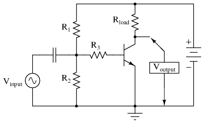
If some percentage of an amplifier’s output signal is connected to the input, so that the amplifier amplifies part of its own output signal, we have what is known as feedback.
Feedback
Feedback comes in two varieties:
- positive (also called regenerative), and
- negative (also called degenerative).
Positive Feedback
Positive feedback reinforces the direction of an amplifier\’s output voltage change, while negative feedback does just the opposite.
A familiar example of feedback happens in public-address (“PA”) systems where someone holds the microphone too close to a speaker: a high-pitched “whine” or “howl” ensues, because the audio amplifier system is detecting and amplifying its own noise.
Specifically, this is an example of positive or regenerative feedback, as any sound detected by the microphone is amplified and turned into a louder sound by the speaker, which is then detected by the microphone again, and so on . . . the result being a noise of steadily increasing volume until the system becomes “saturated” and cannot produce any more volume.
One might wonder what possible benefit feedback is to an amplifier circuit, given such an annoying example as PA system “howl.” If we introduce positive, or regenerative, feedback into an amplifier circuit, it has the tendency of creating and sustaining oscillations, the frequency of which determined by the values of components handling the feedback signal from output to input.
This is one way to make an oscillator circuit to produce AC from a DC power supply. Oscillators are very useful circuits, and so feedback has a definite, practical application for us. See “Phase shift oscillator” , Ch 9 for a practical application of positive feedback.
Negative Feedback
Negative feedback, on the other hand, has a “dampening” effect on an amplifier: if the output signal happens to increase in magnitude, the feedback signal introduces a decreasing influence into the input of the amplifier, thus opposing the change in output signal.
While positive feedback drives an amplifier circuit toward a point of instability (oscillations), negative feedback drives it the opposite direction: toward a point of stability.
An amplifier circuit equipped with some amount of negative feedback is not only more stable, but it distorts the input waveform less and is generally capable of amplifying a wider range of frequencies.
The tradeoff for these advantages (there just has to be a disadvantage to negative feedback, right?) is decreased gain. If a portion of an amplifier\’s output signal is “fed back” to the input to oppose any changes in the output, it will require a greater input signal amplitude to drive the amplifier\’s output to the same amplitude as before.
This constitutes a decreased gain. However, the advantages of stability, lower distortion, and greater bandwidth are worth the tradeoff in reduced gain for many applications.
Common-emitter amplifier without feedback
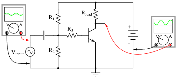
Let\’s examine a simple amplifier circuit and see how we might introduce negative feedback into it, starting with Figure below.
Common-emitter amplifier without feedback.
The amplifier configuration shown here is a common-emitter, with a resistor bias network formed by R1 and R2. The capacitor couples Vinput to the amplifier so that the signal source doesn\’t have a DC voltage imposed on it by the R1/R2 divider network.
Resistor R3 serves the purpose of controlling voltage gain. We could omit it for maximum voltage gain, but since base resistors like this are common in common-emitter amplifier circuits, we\’ll keep it in this schematic.
Like all common-emitter amplifiers, this one inverts the input signal as it is amplified. In other words, a positive-going input voltage causes the output voltage to decrease, or move toward negative, and vice versa. The oscilloscope waveforms are shown in Figure below.
Common-emitter amplifier, no feedback, with reference waveforms for comparison.
Negative feedback in Amplifiers
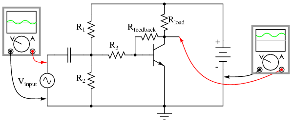
Because the output is an inverted, or mirror-image, reproduction of the input signal, any connection between the output (collector) wire and the input (base) wire of the transistor in Figure below will result in negative feedback.
Negative feedback, collector feedback, decreases the output signal.
The resistances of R1, R2, R3, and Rfeedback function together as a signal-mixing network so that the voltage seen at the base of the transistor (with respect to ground) is a weighted average of the input voltage and the feedback voltage, resulting in signal of reduced amplitude going into the transistor.
So, the amplifier circuit in Figure above will have reduced voltage gain, but improved linearity (reduced distortion) and increased bandwidth.
Emitter feedback
A resistor connecting collector to base is not the only way to introduce negative feedback into this amplifier circuit, though.
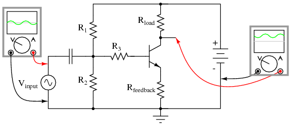
Another method, although more difficult to understand at first, involves the placement of a resistor between the transistor\’s emitter terminal and circuit ground in Figure below.
Emitter feedback: A different method of introducing negative feedback into a circuit.
This new feedback resistor drops voltage proportional to the emitter current through the transistor, and it does so in such a way as to oppose the input signal\’s influence on the base-emitter junction of the transistor.
Let\’s take a closer look at the emitter-base junction and see what difference this new resistor makes in Figure below.
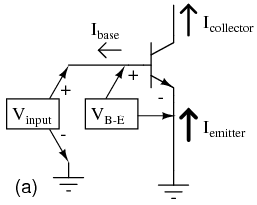
With no feedback resistor connecting the emitter to ground in Figure below (a) , whatever level of input signal (Vinput) makes it through the coupling capacitor and R1/R2/R3 resistor network will be impressed directly across the base-emitter junction as the transistor\’s input voltage (VB-E).
In other words, with no feedback resistor, VB-E equals Vinput. Therefore, if Vinput increases by 100 mV, then VB-E increases by 100 mV: a change in one is the same as a change in the other, since the two voltages are equal to each other.
No Feedback vs Emitter Feedback
Now let\’s consider the effects of inserting a resistor (Rfeedback) between the transistor\’s emitter lead and ground in Figure below (b).
 |
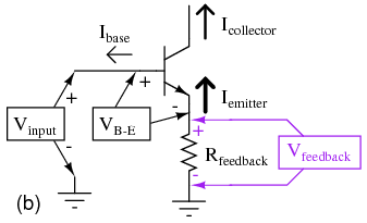 |
(a) No feedback vs (b) emitter feedback. A waveform at the collector is inverted with respect to the base. At (b) the emitter waveform is in-phase (emitter follower) with base, out of phase with collector. Therefore, the emitter signal subtracts from the collector output signal.
Note how the voltage dropped across Rfeedback adds with VB-E to equal Vinput. With Rfeedback in the Vinput — VB-E loop, VB-E will no longer be equal to Vinput. We know that Rfeedback will drop a voltage proportional to emitter current, which is in turn controlled by the base current, which is in turn controlled by the voltage dropped across the base-emitter junction of the transistor (VB-E).
Thus, if Vinput were to increase in a positive direction, it would increase VB-E, causing more base current, causing more collector (load) current, causing more emitter current, and causing more feedback voltage to be dropped across Rfeedback.
This increase of voltage drop across the feedback resistor, though, subtracts from Vinput to reduce the VB-E, so that the actual voltage increase for VB-E will be less than the voltage increase of Vinput.
No longer will a 100 mV increase in Vinput result in a full 100 mV increase for VB-E, because the two voltages are not equal to each other.
Consequently, the input voltage has less control over the transistor than before, and the voltage gain for the amplifier is reduced: just what we expected from negative feedback.
Common-emitter Circuit
In practical common-emitter circuits, negative feedback isn\’t just a luxury; its a necessity for stable operation. In a perfect world, we could build and operate a common-emitter transistor amplifier with no negative feedback, and have the full amplitude of Vinput impressed across the transistor\’s base-emitter junction.
This would give us a large voltage gain. Unfortunately, though, the relationship between base-emitter voltage and base-emitter current changes with temperature, as predicted by the “diode equation.” As the transistor heats up, there will be less of a forward voltage drop across the base-emitter junction for any given current.
This causes a problem for us, as the R1/R2 voltage divider network is designed to provide the correct quiescent current through the base of the transistor so that it will operate in whatever class of operation we desire (in this example, I\’ve shown the amplifier working in class-A mode).
If the transistor\’s voltage/current relationship changes with temperature, the amount of DC bias voltage necessary for the desired class of operation will change. A hot transistor will draw more bias current for the same amount of bias voltage, making it heat up even more, drawing even more bias current. The result, if unchecked, is called thermal runaway.
Common-collector amplifiers
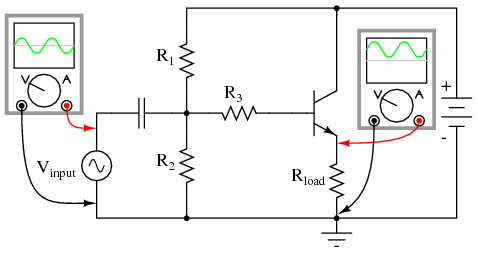
Common-collector amplifiers, (Figure below) however, do not suffer from thermal runaway. Why is this? The answer has everything to do with negative feedback.
Common collector (emitter follower) amplifier.
Note that the common-collector amplifier (Figure above) has its load resistor placed in exactly the same spot as we had the Rfeedback resistor in the last circuit in Figure above (b): between emitter and ground.
This means that the only voltage impressed across the transistor\’s base-emitter junction is the difference between Vinput and Voutput, resulting in a very low voltage gain (usually close to 1 for a common-collector amplifier).
Thermal runaway is impossible for this amplifier: if base current happens to increase due to transistor heating, emitter current will likewise increase, dropping more voltage across the load, which in turn subtracts from Vinput to reduce the amount of voltage dropped between base and emitter.
In other words, the negative feedback afforded by placement of the load resistor makes the problem of thermal runaway self-correcting. In exchange for a greatly reduced voltage gain, we get superb stability and immunity from thermal runaway.
By adding a “feedback” resistor between emitter and ground in a common-emitter amplifier, we make the amplifier behave a little less like an “ideal” common-emitter and a little more like a common-collector. The feedback resistor value is typically quite a bit less than the load, minimizing the amount of negative feedback and keeping the voltage gain fairly high.
Benefits of Negative Feedback
Another benefit of negative feedback, seen clearly in the common-collector circuit, is that it tends to make the voltage gain of the amplifier less dependent on the characteristics of the transistor.
Note that in a common-collector amplifier, voltage gain is nearly equal to unity (1), regardless of the transistor\’s β.
This means, among other things, that we could replace the transistor in a common-collector amplifier with one having a different β and not see any significant changes in voltage gain.
In a common-emitter circuit, the voltage gain is highly dependent on β. If we were to replace the transistor in a common-emitter circuit with another of differing β, the voltage gain for the amplifier would change significantly.
In a common-emitter amplifier equipped with negative feedback, the voltage gain will still be dependent upon transistor β to some degree, but not as much as before, making the circuit more predictable despite variations in transistor β.
The fact that we have to introduce negative feedback into a common-emitter amplifier to avoid thermal runaway is an unsatisfying solution. Is it possibe to avoid thermal runaway without having to suppress the amplifier\’s inherently high voltage gain?
A best-of-both-worlds solution to this dilemma is available to us if we closely examine the problem: the voltage gain that we have to minimize in order to avoid thermal runaway is the DC voltage gain, not the AC voltage gain.
After all, it isn\’t the AC input signal that fuels thermal runaway: its the DC bias voltage required for a certain class of operation: that quiescent DC signal that we use to “trick” the transistor (fundamentally a DC device) into amplifying an AC signal.
We can suppress DC voltage gain in a common-emitter amplifier circuit without suppressing AC voltage gain if we figure out a way to make the negative feedback only function with DC. That is, if we only feed back an inverted DC signal from output to input, but not an inverted AC signal.
The Rfeedback emitter resistor provides negative feedback by dropping a voltage proportional to load current. In other words, negative feedback is accomplished by inserting an impedance into the emitter current path. If we want to feed back DC but not AC, we need an impedance that is high for DC but low for AC. What kind of circuit presents a high impedance to DC but a low impedance to AC? A high-pass filter, of course!
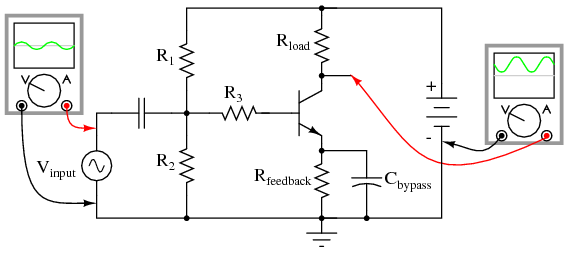
By connecting a capacitor in parallel with the feedback resistor in Figure below, we create the very situation we need: a path from emitter to ground that is easier for AC than it is for DC.
High AC voltage gain reestablished by adding Cbypass in parallel with Rfeedback
The new capacitor “bypasses” AC from the transistor\’s emitter to ground, so that no appreciable AC voltage will be dropped from emitter to ground to “feed back” to the input and suppress voltage gain.
Direct current, on the other hand, cannot go through the bypass capacitor, and so must travel through the feedback resistor, dropping a DC voltage between emitter and ground which lowers the DC voltage gain and stabilizes the amplifier\’s DC response, preventing thermal runaway.
Because we want the reactance of this capacitor (XC) to be as low as possible, Cbypass should be sized relatively large. Because the polarity across this capacitor will never change, it is safe to use a polarized (electrolytic) capacitor for the task.
Another approach to the problem of negative feedback reducing voltage gain is to use multi-stage amplifiers rather than single-transistor amplifiers. If the attenuated gain of a single transistor is insufficient for the task at hand, we can use more than one transistor to make up for the reduction caused by feedback.
Example of Negative Feedback Circuit
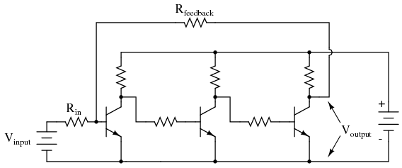
An example circuit showing negative feedback in a three-stage common-emitter amplifier is Figure below.
Feedback around an “odd” number of direct coupled stages produce negative feedback.
The feedback path from the final output to the input is through a single resistor, Rfeedback. Since each stage is a common-emitter amplifier (thus inverting), the odd number of stages from input to output will invert the output signal; the feedback will be negative (degenerative).
Relatively large amounts of feedback may be used without sacrificing voltage gain, because the three amplifier stages provide much gain to begin with.
At first, this design philosophy may seem inelegant and perhaps even counter-productive. Isn\’t this a rather crude way to overcome the loss in gain incurred through the use of negative feedback, to simply recover gain by adding stage after stage?
What is the point of creating a huge voltage gain using three transistor stages if we\’re just going to attenuate all that gain anyway with negative feedback? The point, though perhaps not apparent at first, is increased predictability and stability from the circuit as a whole.
If the three transistor stages are designed to provide an arbitrarily high voltage gain (in the tens of thousands, or greater) with no feedback, it will be found that the addition of negative feedback causes the overall voltage gain to become less dependent of the individual stage gains, and approximately equal to the simple ratio Rfeedback/Rin.
The more voltage gain the circuit has (without feedback), the more closely the voltage gain will approximate Rfeedback/Rin once feedback is established. In other words, voltage gain in this circuit is fixed by the values of two resistors, and nothing more.
This is an advantage for mass-production of electronic circuitry: if amplifiers of predictable gain may be constructed using transistors of widely varied β values, it eases the selection and replacement of components.
It also means the amplifier\’s gain varies little with changes in temperature. This principle of stable gain control through a high-gain amplifier “tamed” by negative feedback is elevated almost to an art form in electronic circuits called operational amplifiers, or op-amps. You may read much more about these circuits in a later chapter of this book!
Review
Feedback is the coupling of an amplifier\’s output to its input.
Positive, or regenerative feedback has the tendency of making an amplifier circuit unstable, so that it produces oscillations (AC). The frequency of these oscillations is largely determined by the components in the feedback network.
Negative, or degenerative feedback has the tendency of making an amplifier circuit more stable, so that its output changes less for a given input signal than without feedback. This reduces the gain of the amplifier, but has the advantage of decreasing distortion and increasing bandwidth (the range of frequencies the amplifier can handle).
Negative feedback may be introduced into a common-emitter circuit by coupling collector to base, or by inserting a resistor between emitter and ground.
An emitter-to-ground “feedback” resistor is usually found in common-emitter circuits as a preventative measure against thermal runaway.
Negative feedback also has the advantage of making amplifier voltage gain more dependent on resistor values and less dependent on the transistor\’s characteristics.
Common-collector amplifiers have much negative feedback, due to the placement of the load resistor between emitter and ground. This feedback accounts for the extremely stable voltage gain of the amplifier, as well as its immunity against thermal runaway.
Voltage gain for a common-emitter circuit may be re-established without sacrificing immunity to thermal runaway, by connecting a bypass capacitor in parallel with the emitter “feedback resistor.”
If the voltage gain of an amplifier is arbitrarily high (tens of thousands, or greater), and negative feedback is used to reduce the gain to reasonable levels, it will be found that the gain will approximately equal Rfeedback/Rin. Changes in transistor β or other internal component values will have little effect on voltage gain with feedback in operation, resulting in an amplifier that is stable and easy to design.
