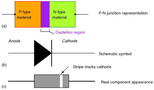
In addition to forward voltage drop (Vf) and peak inverse voltage (PIV), there are many other ratings of diodes important to circuit design and component selection.
Datasheets
Semiconductor manufacturers provide detailed specifications on their products — diodes included — in publications known as datasheets.
Datasheets for a wide variety of semiconductor components may be found in reference books and on the internet. I prefer the internet as a source of component specifications because all the data obtained from manufacturer websites are up-to-date.
Diode Ratings
A typical diode datasheet will contain figures for the following parameters:
Maximum repetitive reverse voltage
VRRM, the maximum amount of voltage the diode can withstand in reverse-bias mode, in repeated pulses. Ideally, this figure would be infinite.
Maximum DC reverse voltage
VR or VDC, the maximum amount of voltage the diode can withstand in reverse-bias mode on a continual basis. Ideally, this figure would be infinite.
Maximum forward voltage
VF, usually specified at the diode’s rated forward current. Ideally, this figure would be zero: the diode providing no opposition whatsoever to forward current. In reality, the forward voltage is described by the “diode equation.”
Maximum (average) forward current
IF(AV), the maximum average amount of current the diode is able to conduct in forward bias mode. This is fundamentally a thermal limitation: how much heat can the PN junction handle, given that dissipation power is equal to current (I) multiplied by voltage (V or E) and forward voltage is dependent upon both current and junction temperature. Ideally, this figure would be infinite.
Maximum (peak or surge) forward current
IFSM or if(surge), the maximum peak amount of current the diode is able to conduct in forward bias mode.
Again, this rating is limited by the diode junction’s thermal capacity, and is usually much higher than the average current rating due to thermal inertia (the fact that it takes a finite amount of time for the diode to reach maximum temperature for a given current). Ideally, this figure would be infinite.
Maximum total dissipation
PD, the amount of power (in watts) allowable for the diode to dissipate, given the dissipation (P=IE) of diode current multiplied by diode voltage drop, and also the dissipation (P=I2R) of diode current squared multiplied by bulk resistance. Fundamentally limited by the diode’s thermal capacity (ability to tolerate high temperatures).
Operating junction temperature
TJ, the maximum allowable temperature for the diode’s PN junction, usually given in degrees Celsius (oC). Heat is the “Achilles’ heel” of semiconductor devices: they must be kept cool to function properly and give long service life.
Storage temperature range
TSTG, the range of allowable temperatures for storing a diode (unpowered). Sometimes given in conjunction with operating junction temperature (TJ), because the maximum storage temperature and the maximum operating temperature ratings are often identical.
If anything, though, maximum storage temperature rating will be greater than the maximum operating temperature rating.
Thermal resistance
R(Θ), the temperature difference between junction and outside air (R(Θ)JA) or between junction and leads (R(Θ)JL) for a given power dissipation.
Expressed in units of degrees Celsius per watt (oC/W). Ideally, this figure would be zero, meaning that the diode package was a perfect thermal conductor and radiator, able to transfer all heat energy from the junction to the outside air (or to the leads) with no difference in temperature across the thickness of the diode package.
A high thermal resistance means that the diode will build up excessive temperature at the junction (where its critical) despite best efforts at cooling the outside of the diode, and thus will limit its maximum power dissipation.
Maximum reverse current
IR, the amount of current through the diode in reverse-bias operation, with the maximum rated inverse voltage applied (VDC).
Sometimes referred to as leakage current. Ideally, this figure would be zero, as a perfect diode would block all current when reverse-biased. In reality, it is very small compared to the maximum forward current.
Typical junction capacitance
CJ, the typical amount of capacitance intrinsic to the junction, due to the depletion region acting as a dielectric separating the anode and cathode connections.
This is usually a very small figure, measured in the range of picofarads (pF).
Reverse recovery time
trr, the amount of time it takes for a diode to “turn off” when the voltage across it alternates from forward-bias to reverse-bias polarity. Ideally, this figure would be zero: the diode halting conduction immediately upon polarity reversal. For a typical rectifier diode, reverse recovery time is in the range of tens of microseconds; for a “fast switching” diode, it may only be a few nanoseconds.
Most of these parameters vary with temperature or other operating conditions, and so a single figure fails to fully describe any given rating. Therefore, manufacturers provide graphs of component ratings plotted against other variables (such as temperature), so that the circuit designer has a better idea of what the device is capable of.

