Printed circuit board (PCB) manufacture is a multi-step process that starts with design and ends with the finished electronic device. Don’t understand the humble PCB board? Producing of a board as small as a few square centimeters involves a number of intricate processing stages, and different PCB board types such as single, double, and multi-layer PCBs also require distinct production techniques. Production issues with PCB board may arise if a stage in the PCB manufacturing process is overlooked.
Moreover, the following section delves into a comprehensive array of terms associated with PCB design, encompassing aspects of manufacturing methods, processes, assembly, and testing. By exploring the terminology on the subsequent page, you’ll gain a deeper insight into the intricacies of printed circuit boards.
PCB Manufactured
In this segment, we explore three distinct varieties of PCBs, detailing their respective manufacturing processes:
- Multilayer PCB
- Double layer PCB
- Single layer PCB
Multi-layer PCB and its manufacturing process
What is a multilayer PCB?
A circuit board with three or more layers of conductive copper foil is referred to as a multilayer PCB. A minimum of three layers of copper are buried in the middle of the dielectric (FR4 material is the most standard one) are required for all multilayer PCBs.
Multi-layer PCB is designed to achieve more functions in a small PCB, it is lighter and smaller than single-layer PCB with the same electronic functions.
Multilayer PCBs are extensively employed in industries such as industrial equipment, automation and control, automotive electronics, new energy, medical equipment, consumer electronics and telecommunications due to their high assembly density design options.
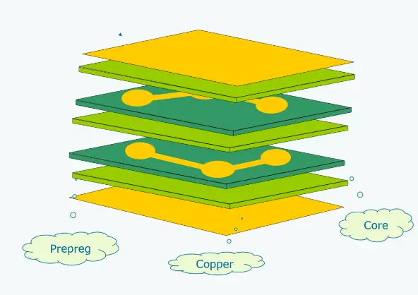
Fig 1. Multilayer PCB
How are multilayer PCBs made?
Here is a process flowchart and a detailed discussion of the multilayer PCB manufacturing process.
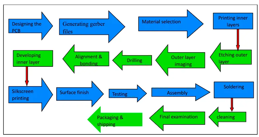
Fig 2. Manufacturing process of multilayer PCB
Designing The PCB: The PCB is designed using dedicated software such as Eagle, Altium, Proteus, Protel, KiCad, Cadence OrCAD PCB Designer, etc. Component location, trace routing, and other details are all part of the design.
Generating Gerber File: Gerber files are produced when the design is finished. The PCB copper layers, copper traces, solder masks, silkscreen, outline and other pertinent information are all in the Gerber files.
Material Selection: Determine the kind of PCB substrate material. For instance, FR-4(Flame Retardant 94v-0), an epoxy laminate reinforced with fiberglass, is a common material. Besides, polyimide, metal, ceramic, and PTEF materials are also used in different PCBs.
Printing Inner Layers: A stack of laminate layers covered in copper is the initial state of the PCB. A substance known as photoresist, which is photosensitive, is applied to the inner layer. The regions where copper should stay are made visible by the Gerber files.
Developing Inner Layers: Copper traces are left on the inner layers after the exposed copper is etched away. After removing the leftover photoresist, the inner layers are cleaned.
Layer Alignment And Bonding: After aligning the inner layers, prepreg layers- layers of fiberglass that have been resin-impregnated- are put in between. After that, pressure and heat are applied to fuse the entire stack together.
Drilling: The PCB is drilled with holes for components and vias. In order to provide electrical connections between layers, copper plating is done to these holes.
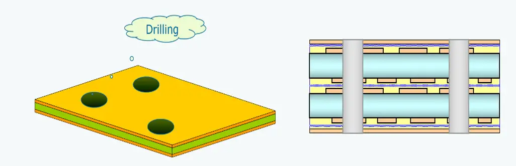
Fig 3. Drilling
The ability for one layer of the printed circuit board to link to another is required for each layer, and this is accomplished by drilling tiny holes known as “VIAS.” An automated drilling machine is typically used to accomplish the precise positioning of the drilled holes.
Numerically controlled drill, or NCD files also known as excellon files are computer programs and files that operate these devices. The drill size and location within the design are established by these files.
Instead of drilling through every layer of the circuit board, one layer can be drilled using controlled depth drilling. Drilling each of the PCB’s individual sheets or layers before lamination can achieve this. Laser drill is also used to produce high-tech HDI circuit boards.
Outer layer imaging: The PCB is exposed to UV light through a mask after the outside layers have been covered with photosensitive material, which defines the outer layer circuitry.
Etching of the outer layers: The circuit traces and pads are left in place after the exposed copper selective curing of the solder mask leaves just the required parts exposed.
Solder mask printing: A layer of solder resistance materials is printed on the PCB surface to protect the copper trace and also avoid solder on the copper in the PCB assembly process.
Silkscreen printing: A technique known as silk screen printing is used to create a coating of white ink for component labelling and reference designators.
Surface finish: The PCBs’ surface is treated to guarantee solderability and shield it from the elements. HASL(Hot Air Solder Leveling), ENIG(Electroless Nickel Immersion Gold), and OSP(Organic Solderability Preservative) are examples of common surface treatments.
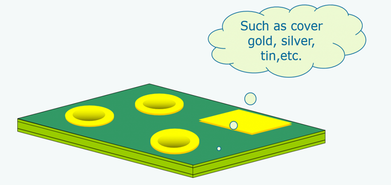
Fig 4. Surface finish
Testing: Electrical testing is done on PCBs to make sure there are no open or short connections. Flying probe testing and fixture testing are usually used for this.
PCB assembly – component insertion: Automated pick-and-place machines are used to place components on the PCB. Surface-mount technology or through-hole technology can be used for the assembling process. For PTH components, manual insertion is always needed.
PCB assembly – Soldering: Wave soldering (for through-hole components) or reflow soldering (for surface-mount components) are the two methods used to solder components to the pads on the PCB.
Cleaning: To get rid of any soldering residue or any dust or stains, the PCB is cleaned.
Final examination: To make sure that all components are soldered and positioned correctly and that there are no flaws, the finished PCBs are subjected to a final examination, such as ICT testing and functional testing. Functional testing is the most reliable test to ensure perfect quality.
Packaging and shipping: After the PCBs are completed, they are packed and ready to be shipped to the final customer or electronic manufacturing service plant for a complete electronic device assembly. PCBs need to be placed in ESD bags and protected in good condition to avoid damage in transportation.
Double-Layer PCB And its manufacturing process
What is a double-layer PCB?
A double-sided printed circuit board also referred to as a two-layer PCB. Double-sided plated through PCB is a kind of PCB with two copper layers that are connected by plated through holes.
Currently, double-sided printed circuit boards (PCBs) are the most widely used printed circuit boards in the electronic industry, such as power PCBs, control PCBs, LED PCBs and many kinds of consumer and industrial electronics.
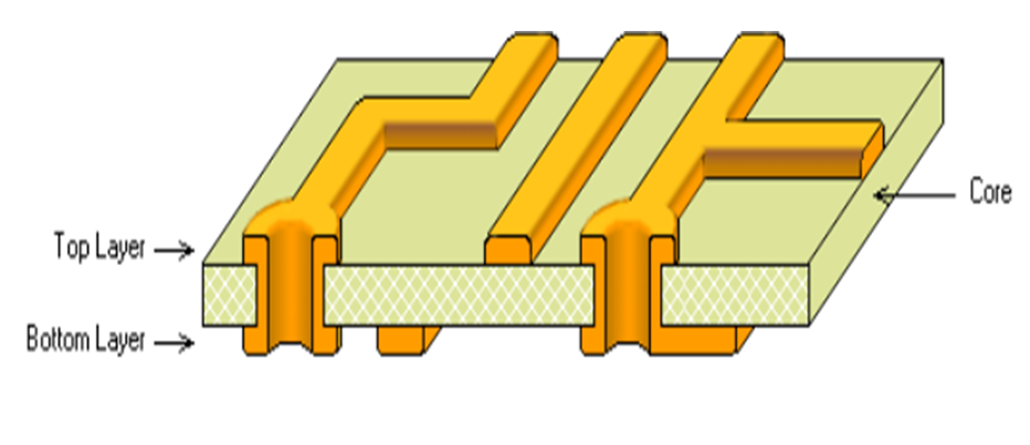
Fig 5. Double layer PCB
How to make a double-layer PCB?
Here is a detailed flowchart of the double layer PCB manufacturing process.
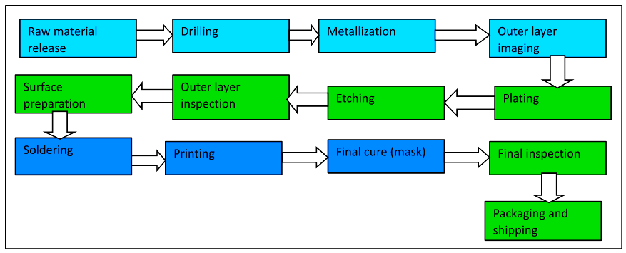
Fig 6. Manufacturing process of Double layer PCB
Single Layer PCB its manufacturing process?
What is a Single Layer PCB?
Because they are so easy to make and low cost, single-layer PCBs are widely used in consumer electronics such as LEDs, TVs, refrigerators, cookers, etc.
A single layer printed circuit board also referred to as a single sided PCB or a one layer PCB, is a form of PCB in which components are placed on one side (a single layer conductive pattern) and conductive copper is utilized on the opposite side to add additional electronic components to the boards’ superiority.
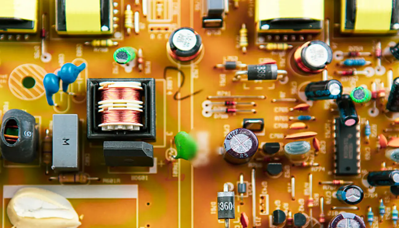
Fig7. Single layer PCB
How to make a single layer PCB?
Here is a detailed flowchart of the single layer PCB manufacturing process.
Fig8. Manufacturing process of single layer PCB
Conclusion
An outline of the important steps in the PCB manufacturing process is given in this step-by-step tutorial. To create PCB boards of the highest quality then each stage necessitates accuracy and focus on detail such as copper etching, laminating, drilling, plating, profiling and surface treatment. It is abundantly evident from the foregoing description that the PCB manufacturing process requires very advanced equipment and very skilled personnel.
Understanding the intricacies of this procedure and the purpose of every stage helps you to understand better the steps, expense, effort, and time required to fabrication and assemble a circuit board. It also helps you to make better choices in designing a new printed circuit board or finding a new PCB supplier.