Serial-in, serial-out shift registers delay data by one clock time for each stage. They will store a bit of data for each register. A serial-in, serial-out shift register may be one to 64 bits in length, longer if registers or packages are cascaded.
Below is a single stage shift register receiving data which is not synchronized to the register clock. The “data in” at the D pin of the type D FF (Flip-Flop) does not change levels when the clock changes for low to high. We may want to synchronize the data to a system wide clock in a circuit board to improve the reliability of a digital logic circuit.
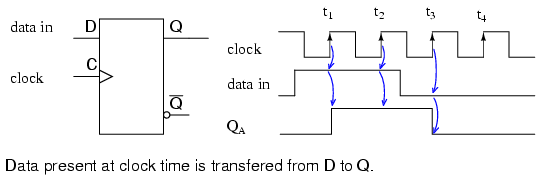
The obvious point (as compared to the figure below) illustrated above is that whatever “data in” is present at the D pin of a type D FF is transfered from D to output Q at clock time.
Since our example shift register uses positive edge sensitive storage elements, the output Q follows the D input when the clock transitions from low to high as shown by the up arrows on the diagram above.
There is no doubt what logic level is present at clock time because the data is stable well before and after the clock edge. This is seldom the case in multi-stage shift registers. But, this was an easy example to start with.
We are only concerned with the positive, low to high, clock edge. The falling edge can be ignored. It is very easy to see Q follow D at clock time above. Compare this to the diagram below where the “data in” appears to change with the positive clock edge.
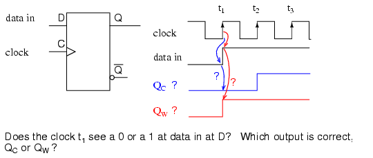
Since “data in” appears to changes at clock time t1 above, what does the type D FF see at clock time? The short over simplified answer is that it sees the data that was present at D prior to the clock.
That is what is transfered to Q at clock time t1. The correct waveform is QC. At t1 Q goes to a zero if it is not already zero. The D register does not see a one until time t2, at which time Q goes high.
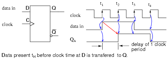
Since data, above, present at D is clocked to Q at clock time, and Q cannot change until the next clock time, the D FF delays data by one clock period, provided that the data is already synchronized to the clock. The QA waveform is the same as “data in” with a one clock period delay.
A more detailed look at what the input of the type D Flip-Flop sees at clock time follows. Refer to the figure below. Since “data in” appears to changes at clock time (above), we need further information to determine what the D FF sees.
If the “data in” is from another shift register stage, another same type D FF, we can draw some conclusions based on data sheet information.
Manufacturers of digital logic make available information about their parts in data sheets, formerly only available in a collection called a data book. Data books are still available; though, the manufacturer\’s web site is the modern source.
The following data was extracted from the CD4006b data sheet for operation at 5VDC, which serves as an example to illustrate timing.
- tS=100ns
- tH=60ns
- tP=200-400ns typ/max
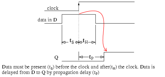
tS is the setup time, the time data must be present before clock time. In this case data must be present at D 100ns prior to the clock. Furthermore, the data must be held for hold time tH=60ns after clock time. These two conditions must be met to reliably clock data from D to Q of the Flip-Flop.
There is no problem meeting the setup time of 60ns as the data at D has been there for the whole previous clock period if it comes from another shift register stage. For example, at a clock frequency of 1 Mhz, the clock period is 1000 µs, plenty of time. Data will actually be present for 1000µs prior to the clock, which is much greater than the minimum required tS of 60ns.
The hold time tH=60ns is met because D connected to Q of another stage cannot change any faster than the propagation delay of the previous stage tP=200ns. Hold time is met as long as the propagation delay of the previous D FF is greater than the hold time. Data at D driven by another stage Q will not change any faster than 200ns for the CD4006b.
To summarize, output Q follows input D at nearly clock time if Flip-Flops are cascaded into a multi-stage shift register.
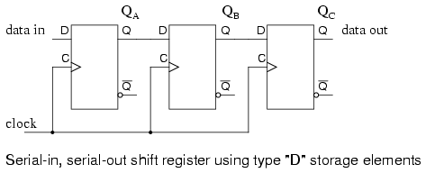
Three type D Flip-Flops are cascaded Q to D and the clocks paralleled to form a three stage shift register above.
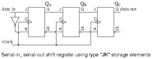
Type JK FFs cascaded Q to J, Q\’ to K with clocks in parallel to yield an alternate form of the shift register above.
A serial-in/serial-out shift register has a clock input, a data input, and a data output from the last stage. In general, the other stage outputs are not available Otherwise, it would be a serial-in, parallel-out shift register..
The waveforms below are applicable to either one of the preceding two versions of the serial-in, serial-out shift register. The three pairs of arrows show that a three stage shift register temporarily stores 3-bits of data and delays it by three clock periods from input to output.
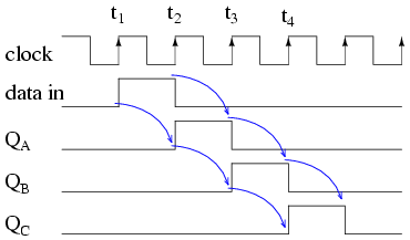
At clock time t1 a “data in” of 0 is clocked from D to Q of all three stages. In particular, D of stage A sees a logic 0, which is clocked to QA where it remains until time t2.
At clock time t2 a “data in” of 1 is clocked from D to QA. At stages B and C, a 0, fed from preceding stages is clocked to QB and QC.
At clock time t3 a “data in” of 0 is clocked from D to QA. QA goes low and stays low for the remaining clocks due to “data in” being 0. QB goes high at t3 due to a 1 from the previous stage. QC is still low after t3 due to a low from the previous stage.
QC finally goes high at clock t4 due to the high fed to D from the previous stage QB. All earlier stages have 0s shifted into them. And, after the next clock pulse at t5, all logic 1s will have been shifted out, replaced by 0s
Serial-in/serial-out devices
We will take a closer look at the following parts available as integrated circuits, courtesy of Texas Instruments. For complete device data sheets follow the links.
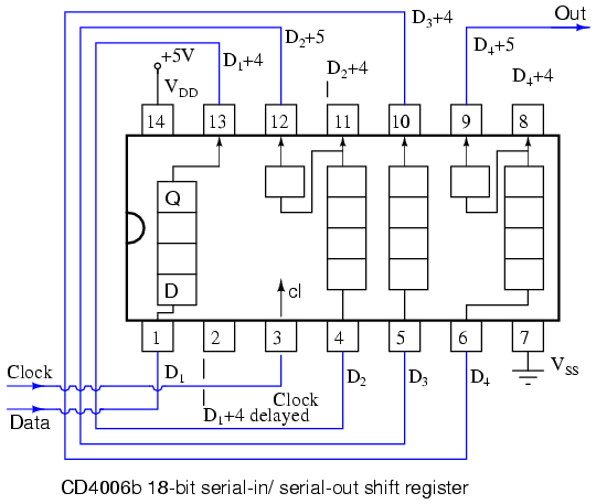
- CD4006b 18-bit serial-in/ serial-out shift register
- CD4031b 64-bit serial-in/ serial-out shift register
- CD4517b dual 64-bit serial-in/ serial-out shift register
The following serial-in/ serial-out shift registers are 4000 series CMOS (Complementary Metal Oxide Semiconductor) family parts. As such, They will accept a VDD, positive power supply of 3-Volts to 15-Volts. The VSS pin is grounded.
The maximum frequency of the shift clock, which varies with VDD, is a few megahertz. See the full data sheet for details.
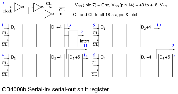
The 18-bit CD4006b consists of two stages of 4-bits and two more stages of 5-bits with a an output tap at 4-bits. Thus, the 5-bit stages could be used as 4-bit shift registers.
To get a full 18-bit shift register the output of one shift register must be cascaded to the input of another and so on until all stages create a single shift register as shown below.
A CD4031 64-bit serial-in/ serial-out shift register is shown below. A number of pins are not connected (nc). Both Q and Q\’ are available from the 64th stage, actually Q64 and Q\’64.
There is also a Q64 “delayed” from a half stage which is delayed by half a clock cycle. A major feature is a data selector which is at the data input to the shift register.
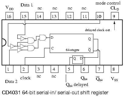
The “mode control” selects between two inputs: data 1 and data 2. If “mode control” is high, data will be selected from “data 2” for input to the shift register. In the case of “mode control” being logic low, the “data 1” is selected.
Examples of this are shown in the two figures below.
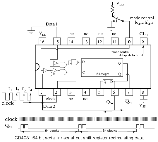
The “data 2” above is wired to the Q64 output of the shift register. With “mode control” high, the Q64 output is routed back to the shifter data input D.
Data will recirculate from output to input. The data will repeat every 64 clock pulses as shown above. The question that arises is how did this data pattern get into the shift register in the first place?
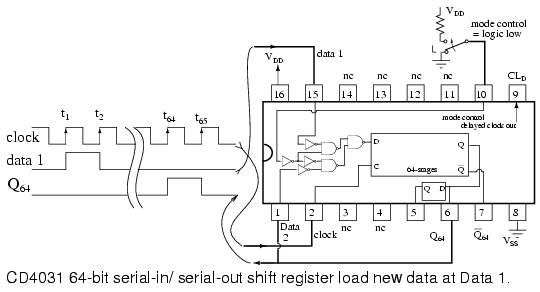
With “mode control” low, the CD4031 “data 1” is selected for input to the shifter. The output, Q64, is not recirculated because the lower data selector gate is disabled.
By disabled we mean that the logic low “mode select” inverted twice to a low at the lower NAND gate prevents it for passing any signal on the lower pin (data 2) to the gate output. Thus, it is disabled.
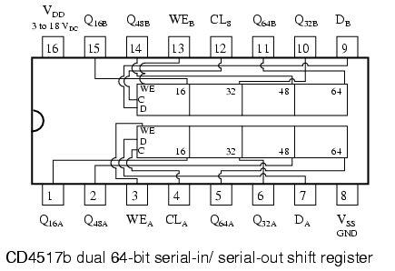
A CD4517b dual 64-bit shift register is shown above. Note the taps at the 16th, 32nd, and 48th stages. That means that shift registers of those lengths can be configured from one of the 64-bit shifters. Of course, the 64-bit shifters may be cascaded to yield an 80-bit, 96-bit, 112-bit, or 128-bit shift register.
The clock CLA and CLB need to be paralleled when cascading the two shifters. WEB and WEB are grounded for normal shifting operations. The data inputs to the shift registers A and B are DA and DB respectively.
Suppose that we require a 16-bit shift register. Can this be configured with the CD4517b? How about a 64-shift register from the same part?
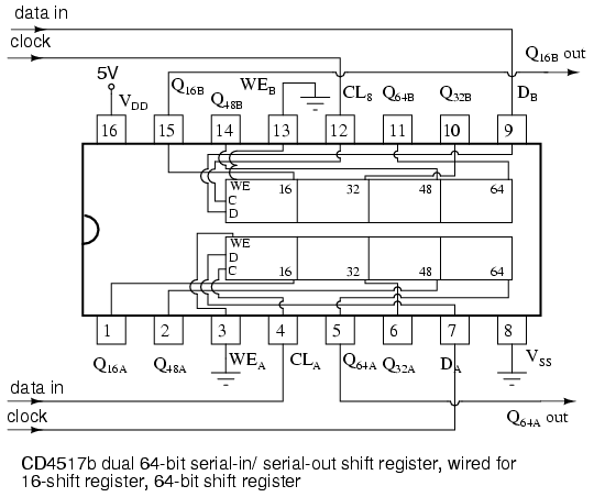
Above we show A CD4517b wired as a 16-bit shift register for section B. The clock for section B is CLB. The data is clocked in at CLB. And the data delayed by 16-clocks is picked of off Q16B. WEB , the write enable, is grounded.
Above we also show the same CD4517b wired as a 64-bit shift register for the independent section A. The clock for section A is CLA. The data enters at CLA. The data delayed by 64-clock pulses is picked up from Q64A. WEA, the write enable for section A, is grounded.
