NAND and NOR gates possess a special property: they are universal. That is, given enough gates, either type of gate is able to mimic the operation of any other gate type.
Universal Gates
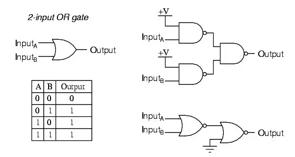
For example, it is possible to build a circuit exhibiting the OR function using three interconnected NAND gates. The ability for a single gate type to be able to mimic any other gate type is one enjoyed only by the NAND and the NOR.
In fact, digital control systems have been designed around nothing but either NAND or NOR gates, all the necessary logic functions being derived from collections of interconnected NANDs or NORs.
As proof of this property, this section will be divided into subsections showing how all the basic gate types may be formed using only NANDs or only NORs.
Constructing the NOT function
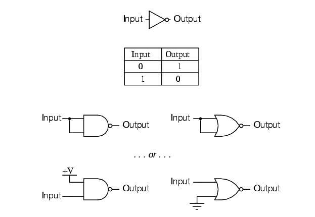
As you can see, there are two ways to use a NAND gate as an inverter, and two ways to use a NOR gate as an inverter. Either method works, although connecting TTL inputs together increases the amount of current loading to the driving gate. For CMOS gates, common input terminals decreases the switching speed of the gate due to increased input capacitance.
Inverters are the fundamental tool for transforming one type of logic function into another, and so there will be many inverters shown in the illustrations to follow.
In those diagrams, I will only show one method of inversion, and that will be where the unused NAND gate input is connected to +V (either Vcc or Vdd, depending on whether the circuit is TTL or CMOS) and where the unused input for the NOR gate is connected to ground.
Bear in mind that the other inversion method (connecting both NAND or NOR inputs together) works just as well from a logical (1’s and 0’s) point of view, but is undesirable from the practical perspectives of increased current loading for TTL and increased input capacitance for CMOS.
Constructing the buffer function
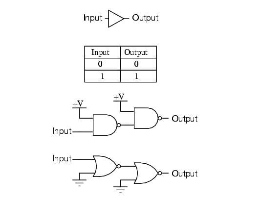
Being that it is quite easy to employ NAND and NOR gates to perform the inverter (NOT) function, it stands to reason that two such stages of gates will result in a buffer function, where the output is the same logical state as the input.
Constructing the AND function
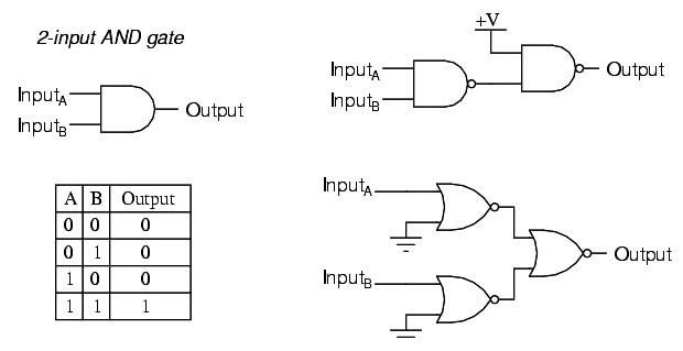
To make the AND function from NAND gates, all that is needed is an inverter (NOT) stage on the output of a NAND gate.
This extra inversion “cancels out” the first N in NAND, leaving the AND function. It takes a little more work to wrestle the same functionality out of NOR gates, but it can be done by inverting (“NOT”) all of the inputs to a NOR gate.
Constructing the NAND function
It would be pointless to show you how to “construct” the NAND function using a NAND gate, since there is nothing to do.
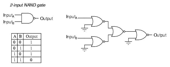
To make a NOR gate perform the NAND function, we must invert all inputs to the NOR gate as well as the NOR gate’s output. For a two-input gate, this requires three more NOR gates connected as inverters.
Constructing the OR function
Inverting the output of a NOR gate (with another NOR gate connected as an inverter) results in the OR function. The NAND gate, on the other hand, requires inversion of all inputs to mimic the OR function, just as we needed to invert all inputs of a NOR gate to obtain the AND function.
Remember that inversion of all inputs to a gate results in changing that gate’s essential function from AND to OR (or vice versa), plus an inverted output.
Thus, with all inputs inverted, a NAND behaves as an OR, a NOR behaves as an AND, an AND behaves as a NOR, and an OR behaves as a NAND. In Boolean algebra, this transformation is referred to as DeMorgan’s Theorem, covered in more detail in a later chapter of this book.
Constructing the NOR function
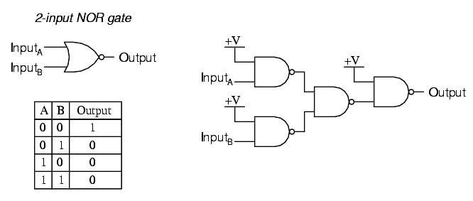
Much the same as the procedure for making a NOR gate behave as a NAND, we must invert all inputs and the output to make a NAND gate function as a NOR.
Review
- NAND and NOR gates are universal: that is, they have the ability to mimic any type of gate, if interconnected in sufficient numbers.
