Inst ToolsInst ToolsInst Tools
  • Courses
  • Automation
    • PLC
    • Control System
    • Safety System
    • Communication
    • Fire & Gas System
  • Instrumentation
    • Design
    • Pressure
    • Temperature
    • Flow
    • Level
    • Vibration
    • Analyzer
    • Control Valve
    • Switch
    • Calibration
    • Erection & Commissioning
  • Interview
    • Instrumentation
    • Electrical
    • Electronics
    • Practical
  • Q&A
    • Instrumentation
    • Control System
    • Electrical
    • Electronics
    • Analog Electronics
    • Digital Electronics
    • Power Electronics
    • Microprocessor
  • Request
Search
  • Books
  • Software
  • Projects
  • Process
  • Tools
  • Basics
  • Formula
  • Power Plant
  • Root Cause Analysis
  • Electrical Basics
  • Animation
  • Standards
  • 4-20 mA Course
  • Siemens PLC Course
Reading: Working of NPN Transistor
Share
Font ResizerAa
Inst ToolsInst Tools
Font ResizerAa
  • Courses
  • Design
  • PLC
  • Interview
  • Control System
Search
  • Courses
  • Automation
    • PLC
    • Control System
    • Safety System
    • Communication
    • Fire & Gas System
  • Instrumentation
    • Design
    • Pressure
    • Temperature
    • Flow
    • Level
    • Vibration
    • Analyzer
    • Control Valve
    • Switch
    • Calibration
    • Erection & Commissioning
  • Interview
    • Instrumentation
    • Electrical
    • Electronics
    • Practical
  • Q&A
    • Instrumentation
    • Control System
    • Electrical
    • Electronics
    • Analog Electronics
    • Digital Electronics
    • Power Electronics
    • Microprocessor
  • Request
Follow US
All rights reserved. Reproduction in whole or in part without written permission is prohibited.
Inst Tools > Blog > Electronic Devices & Circuits > Working of NPN Transistor

Working of NPN Transistor

Last updated: September 27, 2016 4:02 pm
Editorial Staff
Electronic Devices & Circuits
No Comments
Share
5 Min Read
SHARE

The emitter-base junction of a transistor is forward biased whereas collector-base junction is reverse biased. If for a moment, we ignore the presence of emitter-base junction, then practically (Note 1) no current would flow in the collector circuit because of the reverse bias. However, if the emitter-base junction is also present, then forward bias on it causes the emitter current to flow. It is seen that this emitter current almost entirely flows in the collector circuit. Therefore, the current in the collector circuit depends upon the emitter current. If the emitter current is zero, then collector current is nearly zero. However, if the emitter current is 1mA, then collector current is also about 1mA. This is precisely what happens in a transistor. We shall now discuss this transistor action for npn & pnp transistors.

Working of npn transistor

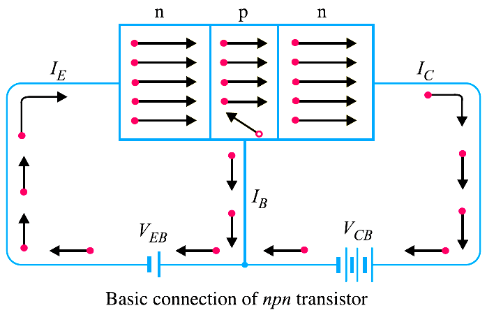
The Below Fig shows the npn transistor with forward bias to emitter-base junction and reverse bias to collector-base junction. The forward bias causes the electrons in the n-type emitter to flow towards the base. This constitutes the emitter current IE. As these electrons flow through the p-type base, they tend to combine with holes. As the base is lightly doped and very thin, therefore, only a few electrons (less than 5%) combine with holes to constitute base (note 2) current IB. The remainder ( (Note 3) more than 95%) cross over into the collector region to constitute collector current IC. In this way, almost the entire emitter current flows in the collector circuit. It is clear that emitter current is the sum of collector and base currents i.e.

IE  = IB + IC

working-of-npn-transistor

Note:

  1. In actual practice, a very little current (a few µA) would flow in the collector circuit. This is called collector cut off current and is due to minority carriers.
  2. The electrons which combine with holes become valence electrons. Then as valence electrons, they flow down through holes and into the external base lead. This constitutes base current IB.
  3. The reasons that most of the electrons from emitter continue their journey through the base to collector to form collector current are : (i) The base is lightly doped and very thin. Therefore, there are a few holes which find enough time to combine with electrons. (ii) The reverse bias on collector is quite high and exerts attractive forces on these electrons.

Working of PNP transistor

The below Fig shows the basic connection of a pnp transistor. The forward bias causes the holes in the p-type emitter to flow towards the base. This constitutes the emitter current IE. As these holes cross into n-type base, they tend to combine with the electrons. As the base is lightly doped and very thin, therefore, only a few holes (less than 5%) combine with the electrons. The remainder (more than 95%) cross into the collector region to constitute collector current IC. In this way, almost the entire emitter current flows in the collector circuit. It may be noted that current conduction within pnp transistor is by holes. However, in the external connecting wires, the current is still by electrons.

working-of-pnp-transistor

Importance of transistor action

The input circuit (i.e. emitter-base junction) has low resistance because of forward bias whereas output circuit (i.e. collector-base junction) has high resistance due to reverse bias. As we have seen, the input emitter current almost entirely flows in the collector circuit. Therefore, a transistor transfers the input signal current from a low-resistance circuit to a high-resistance circuit. This is the key factor responsible for the amplifying capability of the transistor.

Don't Miss Our Updates
Be the first to get exclusive content straight to your email.
We promise not to spam you. You can unsubscribe at any time.
Invalid email address
You've successfully subscribed !

Continue Reading

Basics of Voltage Regulators
Full Wave Rectifier
Transistor as an Amplifier in Common Emitter
Types of Resistors
Permanent Magnet Moving Coil Instruments (PMMC)
What is a Filter Circuit ?
Share This Article
Facebook Whatsapp Whatsapp LinkedIn Copy Link
Share
Leave a Comment

Leave a Reply Cancel reply

Your email address will not be published. Required fields are marked *

Stay Connected

128.3kFollowersLike
69.1kFollowersFollow
210kSubscribersSubscribe
38kFollowersFollow

Categories

Explore More

Photodiode Working Principle
Zener Diode Breakdown Characteristics
Operation of Zener Diode Voltage Regulator
Diodes Voltage Quadrupler
PMMC Temperature Compensation
Light Emitting Diode Operation
Optocouplers Working Principle
Ideal Diode Characteristics

Keep Learning

Comparison of MOSFET and BJT

Comparison of MOSFET and BJT

Cathode Ray Tube (CRT)

Cathode Ray Tube (CRT)

reverse-biased varactor diode

Varactor Diode Operation

Electronic Symbols List

Electronic Symbols

principle of time base generator

Time Base Generator

Transistor Collector Feedback Bias

Transistor Collector Feedback Bias

diode-basic-structure-symbol

Forward Bias & Reverse Bias of a Diode

Field Instruments Questions and Answers

Basics of Amplifiers Interview Questions

Learn More

Differences Between AC and DC Motors

Design & Construction of Process Plant

Process Control Systems Philosophy Concept

PLC Program for Daily Production Record

PLC Program for Daily Production Record

Closed Loop Control System

Types of Control Systems

What is Barring Gear Logic? Why is it Required in the Steam Turbine?

Vortex Flow Meter Principle

Vortex Flow meter Animation

Power Transmission And Distribution

Electrical Power Transmission And Distribution

Vibration Analysis

Top 100 Vibration Analysis Questions and Answers

Menu

  • About
  • Privacy Policy
  • Copyright

Quick Links

  • Learn PLC
  • Helping Hand
  • Part Time Job

YouTube Subscribe

Follow US
All rights reserved. Reproduction in whole or in part without written permission is prohibited.
Welcome Back!

Sign in to your account

Username or Email Address
Password

Lost your password?