Inst ToolsInst ToolsInst Tools
  • Courses
  • Automation
    • PLC
    • Control System
    • Safety System
    • Communication
    • Fire & Gas System
  • Instrumentation
    • Design
    • Pressure
    • Temperature
    • Flow
    • Level
    • Vibration
    • Analyzer
    • Control Valve
    • Switch
    • Calibration
    • Erection & Commissioning
  • Interview
    • Instrumentation
    • Electrical
    • Electronics
    • Practical
  • Q&A
    • Instrumentation
    • Control System
    • Electrical
    • Electronics
    • Analog Electronics
    • Digital Electronics
    • Power Electronics
    • Microprocessor
  • Request
Search
  • Books
  • Software
  • Projects
  • Process
  • Tools
  • Basics
  • Formula
  • Power Plant
  • Root Cause Analysis
  • Electrical Basics
  • Animation
  • Standards
  • 4-20 mA Course
  • Siemens PLC Course
Reading: Power MOSFET
Share
Font ResizerAa
Inst ToolsInst Tools
Font ResizerAa
  • Courses
  • Design
  • PLC
  • Interview
  • Control System
Search
  • Courses
  • Automation
    • PLC
    • Control System
    • Safety System
    • Communication
    • Fire & Gas System
  • Instrumentation
    • Design
    • Pressure
    • Temperature
    • Flow
    • Level
    • Vibration
    • Analyzer
    • Control Valve
    • Switch
    • Calibration
    • Erection & Commissioning
  • Interview
    • Instrumentation
    • Electrical
    • Electronics
    • Practical
  • Q&A
    • Instrumentation
    • Control System
    • Electrical
    • Electronics
    • Analog Electronics
    • Digital Electronics
    • Power Electronics
    • Microprocessor
  • Request
Follow US
All rights reserved. Reproduction in whole or in part without written permission is prohibited.
Inst Tools > Blog > Electronic Devices & Circuits > Power MOSFET

Power MOSFET

Last updated: October 6, 2016 7:30 am
Editorial Staff
Electronic Devices & Circuits
1 Comment
Share
3 Min Read
SHARE

A metal-oxide-semiconductor field-effect transistor(MOSFET) is developed by combining the areas of field-effect concept and MOS technology.

The Conventional planar MOSFET has the restriction of handling the high power. In high power applications, the Double-diffused vertical MOSFET or VMOS is used which is simply known as Power MOSFET.

What is Power MOSFET?

The Power MOSFET is the three terminal (Gate, Drain and Source), four layer (n+pn–n+),Unipolar ( only majority carriers in conduction) semiconductor device. 

  • The MOSFET is a majority carrier device, and as the majority carriers have no recombination delays, the MOSFET achieves extremely high bandwidths and switching times.
  • The gate is electrically isolated from the source, and while this provides the MOSFET with its high input  impedance, it also forms a good capacitor.
  • MOSFETs do not have secondary breakdown area, their drain to source resistance has a positive temperature coefficient, so they tend to be self protective.
  • It has very low ON resistance and no junction voltage drop when forward biased. These features make MOSFET an extremely attractive power supply switching device.

MOSFET Symbol:

N-channel_mosfet_symbol
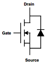
The symbol for n-channel MOSFET is given below. The direction of the arrow on the lead that goes to the body region indicates the direction of current flow. As this is the symbol for n channel MOSFET, the arrow is inwards. For p-channel MOSFET, the arrow will be towards outside.

MOSFET Structure:

MOSFET Structure

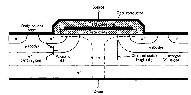
  • The Power MOSFET has a vertically oriented four layer structure of alternating P and N type(n+pn–n+) layers.
  • The P type middle layer is called as body of MOSFET. In this region , the channel is formed between source and drain.
  • The n- layer is called as drift region,which determines the breakdown voltage of the device. This n- region is present only in Power MOSFETs not in signal level MOSFET.
  • The gate terminal is isolated from body by silicon dioxide layer.
  • When the positive gate voltage is applied with respect to source, the n-type channel is formed between source to drain.
  • As shown in the figure, there is a parasitic npn BJT between source and drain.
  • To avoid this BJT turns on, the p-type body region is shorted to source region by overlapping the source metallization on to the p type body.
  • The result is a parasitic diode which is formed between drain to source terminals. This integral diode plays an important role in half and full bridge converter circuits.

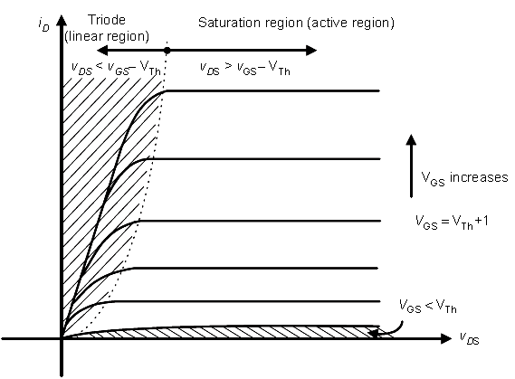
MOSFET VI Characteristics:

The VI characteristics of n-channel enhancement mode MOSFET.

MOSFET VI Characteristics

Don't Miss Our Updates
Be the first to get exclusive content straight to your email.
We promise not to spam you. You can unsubscribe at any time.
Invalid email address
You've successfully subscribed !

Continue Reading

Electronic Symbols
Comparison of Half wave Rectifiers and Full wave Rectifiers
Phototransistor Working Principle
Transistor as a Switch Working Principle
Seven Segment Display Working Principle
Schottky Diode Working Principle
Share This Article
Facebook Whatsapp Whatsapp LinkedIn Copy Link
Share
1 Comment
  • Basavaraju.M.N. says:
    February 25, 2024 at 6:13 pm

    What is the function of field oxide and what is that material?

    Reply

Leave a Reply Cancel reply

Your email address will not be published. Required fields are marked *

Stay Connected

128.3kFollowersLike
69.1kFollowersFollow
210kSubscribersSubscribe
38kFollowersFollow

Categories

Explore More

Forward Bias & Reverse Bias of a Diode
Full Wave Voltage Doubler using Diodes
VI Characteristic of a Diode
Resistors Principle & Applications
Varactor Diode Operation
Combining Independent Voltage Sources in Series
Difference between ideal diode & conventional diode
Basic Transistor Amplifier Circuit Principle

Keep Learning

example-of-KCL

What is Kirchhoff’s Current Law

working-of-pnp-transistor

Working of NPN Transistor

Reverse Voltage Characteristics of Photo diode

Characteristics of Photo diode

Zener Diode

Zener Diode Breakdown Characteristics

Types of Resistors

Types of Resistors

Transistors Questions & Answers

Transistors Questions & Answers

Full Wave Bridge Rectifier Operation

Full Wave Bridge Rectifier Operation

principle of time base generator

Time Base Generator

Learn More

parallel-resistors-circuit-example

Series and Parallel Resistors

Zone vs Class - Division

Zone vs Class / Division

Instrumentation Design Details

I&C Engineer Roles & Responsibilities – Instrumentation Design

What is a Differential Mode Signal

Difference Between Differential Mode and Common Mode

Pressure gauge is subjected to five different pressures

How a Bourdon Tube Pressure Gauge might be Adjusted for Linearity?

Optimal Control Systems

Optimal Control Problems – Part 2

Radiochemical Questions and Answers

Fundamentals of Radiochemical Methods Questions

Turbine Flow Meter

All About Turbine Meters

Menu

  • About
  • Privacy Policy
  • Copyright

Quick Links

  • Learn PLC
  • Helping Hand
  • Part Time Job

YouTube Subscribe

Follow US
All rights reserved. Reproduction in whole or in part without written permission is prohibited.
Welcome Back!

Sign in to your account

Username or Email Address
Password

Lost your password?