Logic diagrams have many uses. In the solid state industry, they are used as the principal diagram for the design of solid state components such as computer chips.
They are used by mathematicians to help solve logical problems (called boolean algebra).
However, their principle application at industrial facilities is their ability to present component and system operational information.
The use of logic symbology results in a diagram that allows the user to determine the operation of a given component or system as the various input signals change.
To read and interpret logic diagrams, the reader must understand what each of the specialized symbols represent.
This article discusses the common symbols used on logic diagrams. When mastered, this knowledge should enable the reader to understand most logic diagrams.
Facility operators and technical staff personnel commonly see logic symbols on equipment diagrams.
The logic symbols, called gates, depict the operation/start/stop circuits of components and systems.
Engineering Logic Diagrams
The following two figures, which use a common facility start/stop pump circuit as an example, clearly demonstrate the reasons for learning to read logic diagrams.
Figure 1 presents a schematic for a large pump, and Figure 2 shows the same pump circuit using only logic gates.
It is obvious that when the basic logic symbols are understood, figuring out how the pump operates and how it will respond to various combinations of inputs using the logic diagram is fast and easy, as compared to laboriously tracing through the relays and contacts of the schematic diagram for the same information.

Figure 1 Example of a Pump Start Circuit Schematic Diagram

Figure 2 Example of Figure 1 Pump Start Circuit as a Logic Diagram
Symbology
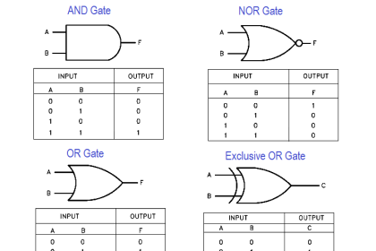
There are three basic types of logic gates. They are AND, OR, and NOT gates. Each gate is a very simple device that only has two states, on and off.
The states of a gate are also commonly referred to as high or low, 1 or 0, or True or False, where on = high = 1 = True, and off = low = 0 = False.
The state of the gate, also referred to as its output, is determined by the status of the inputs to the gate, with each type of gate responding differently to the various possible combinations of inputs.
Specifically, these combinations are as follows.
- AND gate – provides an output (on) when all its inputs are on. When any one of the inputs is off, the gate’s output is off.
- OR gate – provides an output (on) when any one or more of its inputs is on. The gate is off only when all of its inputs are off.
- NOT gate – provides a reversal of the input. If the input is on, the output will be off. If the input is off, the output will be on.
Because the NOT gate is frequently used in conjunction with AND and OR gates, special symbols have been developed to represent these combinations.
The combination of an AND gate and a NOT gate is called a NAND gate. The combination of an OR gate with a NOT gate is called a NOR gate.
- NAND gate – is the opposite (NOT) of an AND gate’s output. It provides an output (on) except when all the inputs are on.
- NOR gate – is the opposite (NOT) of an OR gate’s output. It provides an output only when all inputs are off.
Figure 3 illustrates the symbols covering the three basic logic gates plus NAND and NOR gates. The IEEE/ANSI symbols are used most often; however, other symbol conventions are provided on Figure 3 for information.

Figure 3 Basic Logic Symbols
The AND gate has a common variation called a COINCIDENCE gate. Logic gates are not limited to two inputs.
Theoretically, there is no limit to the number of inputs a gate can have. But, as the number of inputs increases, the symbol must be altered to accommodate the increased inputs.
There are two basic ways to show multiple inputs. Figure 4 demonstrates both methods, using an OR gate as an example.
The symbols used in Figure 4 are used extensively in computer logic diagrams. Process control logic diagrams usually use the symbology shown in Figure 2.
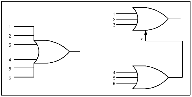
Figure 4 Conventions for Depicting Multiple Inputs
The COINCIDENCE gate behaves like an AND gate except that only a specific number of the total number of inputs needs to be on for the gate’s output to be on. The symbol for a COINCIDENCE gate is shown in Figure 5.
The fraction in the logic symbol indicates that the AND gate is a COINCIDENCE gate.
The numerator of the fraction indicates the number of inputs that must be on for the gate to be on. The denominator states the total number of inputs to the gate.
Figure 5 COINCIDENCE Gate
Two variations of the OR gate are the EXCLUSIVE OR and its opposite, the EXCLUSIVE NOR. The EXCLUSIVE OR and the EXCLUSIVE NOR are symbolized by adding a line on the back of the standard OR or NOR gate’s symbol, as illustrated in Figure 6.
- EXCLUSIVE OR – provides an output (on) when only one of the inputs is on. Any other combination results in no output (off).
- EXCLUSIVE NOR – is the opposite (NOT) of an EXCLUSIVE OR gate’s output. It provides an output only when all inputs are on or when all inputs are off.

Figure 6 EXCLUSIVE OR and EXCLUSIVE NOR Gates
Time Delays
When logic diagrams are used to represent start/stop/operate circuits, the diagrams must also be able to symbolize the various timing devices found in the actual circuits. There are three major types of timers.
They are
- The Type-One Time Delay Device,
- The Type-Two Time Delay Device, and
- The Type-Three Time Delay Device.
Upon receipt of the input signal, the Type-One Time Delay Device delays the output (on) for the specified period of time, but the output will stop (off) as soon as the input signal is removed, as illustrated by Figure 7. The symbol for this type of timer is illustrated in Figure 7.

Figure 7 Type One Time Delay Device
The Type-Two Time Delay Device provides an output signal (on) immediately upon reciept of the input signal, but the output is maintained only for a specified period of time once the input signal (off) has been removed. Figure 8 demonstrates the signal response, and Figure 8 illustrates the symbol used to denote this type of timer.

Figure 8 Type Two Time Delay Device
Upon reciept of an input signal, Type-Three Time Delay Devices provide an output signal for a specified period of time, regardless of the duration of the input. Figure 9 demonstrates the signal response and illustrates the symbol used to denote the timer.

Figure 9 Type-Three Time Delay Device
Complex Logic Devices
In addition to the seven basic logic gates, there are several complex logic devices that may be encountered in the use of logic prints.
Memory devices – In many circuits, a device that can “remember” the last command or the last position is required for a circuit to function.
Like the AND and OR gates, memory devices have been designed to work with on/off signals.
The two input signals to a memory device are called set and reset. Figure 10 shows the common symbols used for memory devices.

Figure 10 Symbols for Complex Logic Devices
Flop-flop – As the name implies, a flip-flop is a device in which as one or more of its inputs changes, the output changes.
A flip-flop is a complex circuit constructed from OR and NOT gates, but is used so frequently in complex circuits that it has its own symbol. Figure 10 shows the common symbol used for a flip-flop.
This device, although occasionally used on component and system type logic diagrams, is principally used in solid state logic diagrams (computers).
Binary counter – Several types of binary counters exist, all of which are constructed of flip-flops. The purpose of a counter is to allow a computer to count higher than 1, which is the highest number a single flip-flop can represent. By ganging flip-flops, higher binary numbers can be constructed. Figure 10 illustrates a common symbol used for a binary counter.
Shift register – Is a storage device constructed of flip-flops that is used in computers to provide temporary storage of a binary word. Figure 10 shows the common symbol used for a shift register.
Half adder – Is a logic circuit that is used in computer circuits to allow the computer to “carry” numbers when it is performing mathematical operations (for example to perform the addition of 9 + 2, a single 10s unit must be “carried” from the ones column to the tens column). Figure 10 illustrates the symbol used for a half adder.