Inst ToolsInst ToolsInst Tools
  • Courses
  • Automation
    • PLC
    • Control System
    • Safety System
    • Communication
    • Fire & Gas System
  • Instrumentation
    • Design
    • Pressure
    • Temperature
    • Flow
    • Level
    • Vibration
    • Analyzer
    • Control Valve
    • Switch
    • Calibration
    • Erection & Commissioning
  • Interview
    • Instrumentation
    • Electrical
    • Electronics
    • Practical
  • Q&A
    • Instrumentation
    • Control System
    • Electrical
    • Electronics
    • Analog Electronics
    • Digital Electronics
    • Power Electronics
    • Microprocessor
  • Request
Search
  • Books
  • Software
  • Projects
  • Process
  • Tools
  • Basics
  • Formula
  • Power Plant
  • Root Cause Analysis
  • Electrical Basics
  • Animation
  • Standards
  • 4-20 mA Course
  • Siemens PLC Course
Reading: Basics of Transistors
Share
Font ResizerAa
Inst ToolsInst Tools
Font ResizerAa
  • Courses
  • Design
  • PLC
  • Interview
  • Control System
Search
  • Courses
  • Automation
    • PLC
    • Control System
    • Safety System
    • Communication
    • Fire & Gas System
  • Instrumentation
    • Design
    • Pressure
    • Temperature
    • Flow
    • Level
    • Vibration
    • Analyzer
    • Control Valve
    • Switch
    • Calibration
    • Erection & Commissioning
  • Interview
    • Instrumentation
    • Electrical
    • Electronics
    • Practical
  • Q&A
    • Instrumentation
    • Control System
    • Electrical
    • Electronics
    • Analog Electronics
    • Digital Electronics
    • Power Electronics
    • Microprocessor
  • Request
Follow US
All rights reserved. Reproduction in whole or in part without written permission is prohibited.
Inst Tools > Blog > Electronic Devices & Circuits > Basics of Transistors

Basics of Transistors

Last updated: September 27, 2016 4:05 pm
Editorial Staff
Electronic Devices & Circuits
No Comments
Share
5 Min Read
SHARE

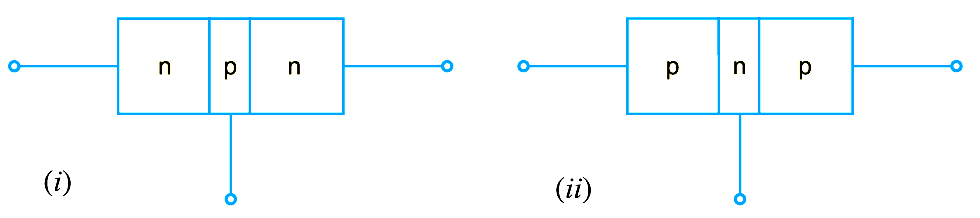
A transistor consists of two pn junctions formed by *sandwiching either p-type or n-type semicon-ductor between a pair of opposite types. Accordingly ; there are two types of transistors, namely;

(i)  n-p-n transistor                                (ii)  p-n-p transistor

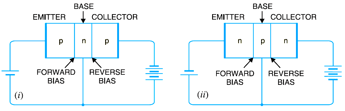
An n–p–n transistor is composed of two n-type semiconductors separated by a thin section of p-type as shown in Fig. (i). However, a p-n-p transistor is formed by two p-sections separated by a thin section of n-type as shown in Fig. (ii).

transistor symbols

In each type of transistor, the following points may be noted :

(i) These are two pn junctions. Therefore, a transistor may be regarded as a combination of two diodes connected back to back.

(ii)  There are three terminals, one taken from each type of semiconductor.

(iii) The middle section is a very thin layer. This is the most important factor in the function of a transistor.

Transistor Terminals

A transistor (pnp or npn) has three sections of doped semiconductors. The section on one side is the emitter and the section on the opposite side is the collector. The middle section is called the base and forms two junctions between the emitter and collector.

(i) Emitter. The section on one side that supplies charge carriers (electrons or holes) is called the emitter. The emitter is always forward biased w.r.t. base so that it can supply a large number of *majority carriers. In Below Fig. (i), the emitter (p-type) of pnp transistor is forward biased and supplies hole charges to its junction with the base. Similarly, in Below Fig. (ii), the emitter (n-type) of npn transistor has a forward bias and supplies free electrons to its junction with the base.

(ii) Collector. The section on the other side that collects the charges is called the collector. The collector is always reverse biased. Its function is to remove charges from its junction with the base. In Below Fig (i), the collector (p-type) of pnp transistor has a reverse bias and receives hole charges that flow in the output circuit. Similarly, in Below Fig. (ii), the collector (n-type) of npn transistor has reverse bias and receives electrons.

(iii) Base. The middle section which forms two pn-junctions between the emitter and collector is called the base. The base-emitter junction is forward biased, allowing low resistance for the emit-ter circuit. The base-collector junction is reverse biased and provides high resistance in the collector circuit.

transistor-terminals

Facts about the Transistor

Before discussing transistor action, it is important that the reader may keep in mind the following facts about the transistor :

(i) The transistor has three regions, namely ; emitter, base and collector. The base is much thinner than the emitter while **collector is wider than both as shown in Fig. However, for the sake of convenience, it is customary to show emitter and collector to be of equal size.

(ii) The emitter is heavily doped so that it can inject a large number of charge carriers (electrons or holes) into the base. The base is lightly doped and very thin ; it passes most of the emitter injected charge carriers to the collector. The collector is moderately doped.

(iii) The transistor has two pn junctions i.e. it is like two diodes. The junction between emitter and base may be called emitter-base diode or simply the emitter diode. The junction between the base and collector may be called collector-base diode or simply collector diode.

(iv) The emitter diode is always forward biased whereas collector diode is always reverse biased.

(v) The resistance of emitter diode (forward biased) is very small as compared to collector diode (reverse biased). Therefore, forward bias applied to the emitter diode is generally very small whereas reverse bias on the collector diode is much higher.

Don't Miss Our Updates
Be the first to get exclusive content straight to your email.
We promise not to spam you. You can unsubscribe at any time.
Invalid email address
You've successfully subscribed !

Continue Reading

Capacitor Filter Working Principle
Transistor Amplifier Working Principle
Freewheeling Diode Working Principle
Schottky Diode Working Principle
pi filter Operation
Basics of Ohm’s Law
Share This Article
Facebook Whatsapp Whatsapp LinkedIn Copy Link
Share
Leave a Comment

Leave a Reply Cancel reply

Your email address will not be published. Required fields are marked *

Stay Connected

128.3kFollowersLike
69.1kFollowersFollow
210kSubscribersSubscribe
38kFollowersFollow

Categories

Explore More

Transistor Collector Feedback Bias
Voltage Divider Rule
Shockley Diode Working Principle
PIN Diode Working Principle
Light Emitting Diode Operation
Transistor Voltage Divider Bias
Semiconductors Diodes Questions & Answers
Comparison of Half wave Rectifiers and Full wave Rectifiers

Keep Learning

Dependent Current Source

Dependent Current Source

Full Wave Rectifier Peak Inverse Voltage

Full Wave Bridge Rectifier Peak Inverse Voltage

Full Wave Rectifier

Full Wave Rectifier

energy-diagrams-for-insulator-semiconductor-and-conductor

Band Gap for Semiconductor Materials

Why Silicon is preferred over Germanium ?

Why Silicon is preferred over Germanium ?

Ideal Diode Characteristics Curve

Difference between ideal diode & conventional diode

Applications of Photo diodes

Applications of Photo diodes

Zener Diode Voltage Regulator Operation

Zener Diode Voltage Regulator Operation

Learn More

Electrical Machines Questions and Answers

Induction Motor Rotor Frequency

AC Generator Nameplate Ratings

AC Generator Nameplate Ratings

Location of Pressure Taps

Design Considerations of Orifice Plate

Control Valve Positioner Working Principle

Control Valve Positioner Working Principle

Power Electronics Objective Questions

Interconnecting Thyristors Objective Questions and Answers

Displacer Level Transmitter weight calibration

Displacer Level Transmitter Dry Calibration with Weights

Fieldbus Flow Transmitter Configuration

Fieldbus Flow Transmitter Configuration

Classification of HVAC chillers

Classification of HVAC Chillers

Menu

  • About
  • Privacy Policy
  • Copyright

Quick Links

  • Learn PLC
  • Helping Hand
  • Part Time Job

YouTube Subscribe

Follow US
All rights reserved. Reproduction in whole or in part without written permission is prohibited.
Welcome Back!

Sign in to your account

Username or Email Address
Password

Lost your password?