Inst ToolsInst ToolsInst Tools
  • Ask
  • Courses
  • Videos
  • Q & A
    • Interview
      • Instrumentation
      • Electronics
      • Electrical
      • Practical Questions
    • MCQ
      • Instrumentation MCQ
      • Electrical MCQ
      • Electronics MCQ
      • Control Systems MCQ
      • Analog Electronics MCQ
      • Digital Electronics MCQ
      • Power Electronics MCQ
      • Microprocessor MCQ
      • Multiple Choice Questions
  • EE
    • Electronics
      • Electronics Q & A
      • Electronic Basics
      • Electronic Devices & Circuits
      • Electronics Animation
      • Digital Electronics
    • Electrical
      • Electrical Basics
      • Electrical Q & A
      • Power Electronics
      • Electrical Machines
      • Electrical Animation
      • Power Systems
      • Switchgear & Protection
      • Transmission & Distribution
  • Measure
    • Control Valves
    • Calibration
    • Temperature
    • Pressure
    • Flow
    • Level
    • Analyzers
    • Switches
    • Vibration
    • Solenoid Valve
  • Control
    • PLC Tutorials
    • Control Systems
    • Safety Instrumented System (SIS)
    • Communication
    • Fire & Gas System
  • More
    • Design
    • Tools
    • Animation
    • Basics
    • Formulas
    • Standards
    • TextBooks
    • Common
    • Software
    • Excel Tools
    • Erection & Commissioning
    • Process Fundamentals
    • Videos
    • Books
Search
All rights reserved. Reproduction in whole or in part without written permission is prohibited.
Reading: Transistor Biasing
Share
Notification Show More
Font ResizerAa
Inst ToolsInst Tools
Font ResizerAa
  • Courses
  • PLC Tutorials
  • Control Systems
Search
  • Ask
  • Courses
  • Videos
  • Q & A
    • Interview
    • MCQ
  • EE
    • Electronics
    • Electrical
  • Measure
    • Control Valves
    • Calibration
    • Temperature
    • Pressure
    • Flow
    • Level
    • Analyzers
    • Switches
    • Vibration
    • Solenoid Valve
  • Control
    • PLC Tutorials
    • Control Systems
    • Safety Instrumented System (SIS)
    • Communication
    • Fire & Gas System
  • More
    • Design
    • Tools
    • Animation
    • Basics
    • Formulas
    • Standards
    • TextBooks
    • Common
    • Software
    • Excel Tools
    • Erection & Commissioning
    • Process Fundamentals
    • Videos
    • Books
Follow US
All rights reserved. Reproduction in whole or in part without written permission is prohibited.
Inst Tools > Blog > Electronic Devices & Circuits > Transistor Biasing

Transistor Biasing

Last updated: September 27, 2016 4:13 pm
Editorial Staff
Electronic Devices & Circuits
No Comments
Share
3 Min Read
SHARE

The below Figure shows a bias arrangement for both npn and pnp BJTs for operation as an amplifier. Notice that in both cases the base-emitter (BE) junction is forward-biased and the base-collector (BC) junction is reverse-biased. This condition is called forward-reverse bias.

Transistor Biasing

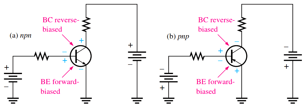
Fig : Forward-reverse bias of a BJT.

Operation :

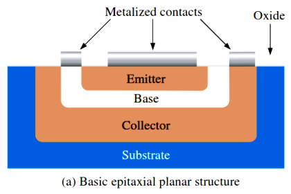
To understand how a transistor operates, let’s examine what happens inside the npn structure. The heavily doped n-type emitter region has a very high density of conduction-band (free) electrons. These free electrons easily diffuse through the forward based BE junction into the lightly doped and very thin p-type base region, as indicated by the wide arrow. The base has a low density of holes, which are the majority carriers, as represented by the white circles. A small percentage of the total number of free electrons injected into the base region recombine with holes and move as valence electrons through the base region and into the emitter region as hole current, indicated by the red arrows.

When the electrons that have recombined with holes as valence electrons leave the crystalline structure of the base, they become free electrons in the metallic base lead and produce the external base current. Most of the free electrons that have entered the base do not recombine with holes because the base is very thin. As the free electrons move toward the reverse-biased BC junction, they are swept across into the collector region by the attraction of the positive collector supply voltage. The free electrons move through the collector region, into the external circuit, and then return into the emitter region along with the base current, as indicated. The emitter current is slightly greater than the collector current because of the small base current that splits off from the total current injected into the base region from the emitter.
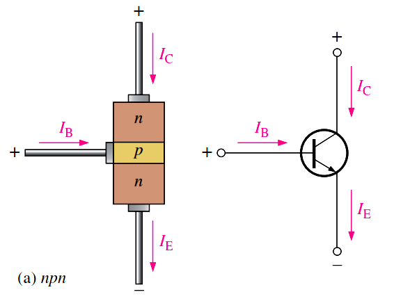
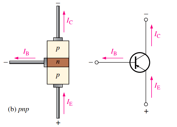
Transistor Currents

The directions of the currents in an npn transistor and its schematic symbol are as shown in Below Figure (a); those for a pnp transistor are shown in Figure Below (b). Notice that the arrow on the emitter inside the transistor symbols points in the direction of conventional current. These diagrams show that the emitter current (IE) is the sum of the collector current (IC) and the base current (IB), expressed as follows:

Transistor Currents

IB is very small compared to IE or IC. The capital-letter subscripts indicate dc values.

npn-transistor-currents

ppn-transistor-currents

Don't Miss Our Updates
Be the first to get exclusive content straight to your email.
We promise not to spam you. You can unsubscribe at any time.
Invalid email address
You've successfully subscribed !
Transistor Stabilisation
Power MOSFET Safe Operating Area
Limitations of Resistors
Dependent Voltage Source
Choke Input Filter Operation
Share This Article
Facebook Whatsapp Whatsapp LinkedIn Copy Link
Share
Leave a Comment

Leave a Reply Cancel reply

Your email address will not be published. Required fields are marked *

Stay Connected

128.3kFollowersLike
69.1kFollowersFollow
208kSubscribersSubscribe
38kFollowersFollow

Categories

Recent Comments

  • Kamli on Top Free PLC Software
  • Guifty Shimica on Top Non-PLC Certification Courses for Automation Professionals
  • Guifty Shimica on Top Non-PLC Certification Courses for Automation Professionals
  • MIHARITSOA Aina Sitraka on Top Non-PLC Certification Courses for Automation Professionals

Related Articles

Full Wave Rectifier Peak Inverse Voltage

Full Wave Bridge Rectifier Peak Inverse Voltage

transistor-base-bias

Transistor Base Bias

seven-segment-display-circuit

Seven Segment Display Working Principle

Zener Diode Limiter Working

Zener Diode Limiter

capacitor-filter-ripples

Ripple Voltage in Rectifiers

Methods of Transistor Biasing

Methods of Transistor Biasing

Photodiode as Variable Resistance Device

Photodiode as Variable Resistance Device

Schottky Diode Vs PN junction Diode

Difference between Schottky Diode and PN junction Diode

More Articles

DeltaV Tune Tutorial

How to Tune a Loop in DeltaV System

Selection Criteria of PH Analyzer

Selection Criteria of pH Analyzers

Sink or source PNP or NPN Normally Open or Normally Closed Input v. output. output

Sink or Source? Normally Open or Normally Closed?

Actuators Questions and Answers

Actuators Questions and Answers

How to Install Thermowell on an Elbow?

Innovative Segment Orifice

Stuck Segment Orifice Dimensions Calculations

Argonite/CO2 Flooding System Master & Slave Cylinder Operation

Applications of CNC Machining

Important Applications of Rapid Prototype CNC Machining Services

Follow US
All rights reserved. Reproduction in whole or in part without written permission is prohibited.
Welcome Back!

Sign in to your account

Username or Email Address
Password

Lost your password?