Inst ToolsInst ToolsInst Tools
  • Courses
  • Automation
    • PLC
    • Control System
    • Safety System
    • Communication
    • Fire & Gas System
  • Instrumentation
    • Design
    • Pressure
    • Temperature
    • Flow
    • Level
    • Vibration
    • Analyzer
    • Control Valve
    • Switch
    • Calibration
    • Erection & Commissioning
  • Interview
    • Instrumentation
    • Electrical
    • Electronics
    • Practical
  • Q&A
    • Instrumentation
    • Control System
    • Electrical
    • Electronics
    • Analog Electronics
    • Digital Electronics
    • Power Electronics
    • Microprocessor
  • Request
Search
  • Books
  • Software
  • Projects
  • Process
  • Tools
  • Basics
  • Formula
  • Power Plant
  • Root Cause Analysis
  • Electrical Basics
  • Animation
  • Standards
  • 4-20 mA Course
  • Siemens PLC Course
Reading: Transistor Load Line Analysis
Share
Font ResizerAa
Inst ToolsInst Tools
Font ResizerAa
  • Courses
  • Design
  • PLC
  • Interview
  • Control System
Search
  • Courses
  • Automation
    • PLC
    • Control System
    • Safety System
    • Communication
    • Fire & Gas System
  • Instrumentation
    • Design
    • Pressure
    • Temperature
    • Flow
    • Level
    • Vibration
    • Analyzer
    • Control Valve
    • Switch
    • Calibration
    • Erection & Commissioning
  • Interview
    • Instrumentation
    • Electrical
    • Electronics
    • Practical
  • Q&A
    • Instrumentation
    • Control System
    • Electrical
    • Electronics
    • Analog Electronics
    • Digital Electronics
    • Power Electronics
    • Microprocessor
  • Request
Follow US
All rights reserved. Reproduction in whole or in part without written permission is prohibited.
Inst Tools > Blog > Electronic Devices & Circuits > Transistor Load Line Analysis

Transistor Load Line Analysis

Last updated: September 27, 2016 2:41 pm
Editorial Staff
Electronic Devices & Circuits
No Comments
Share
4 Min Read
SHARE

In the transistor circuit analysis, it is generally required to determine the collector current for various collector-emitter voltages. One of the methods can be used to plot the output characteristics and determine the collector current at any desired collector-emitter voltage. However, a more convenient method, known as load line method can be used to solve such problems. As explained later in this section, this method is quite easy and is frequently used in the analysis of transistor applications.

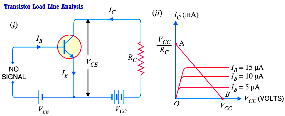
d.c. load line. Consider a common emitter npn transistor circuit shown in Fig. (i) where no signal is applied. Therefore, d.c. conditions prevail in the circuit. The output characteristics of this circuit are shown in Fig. (ii).

The value of collector-emitter voltage VCE at any time is given by ;

VCE     = VCC – IC RC

Transistor Load Line Analysis

As VCC and RC are fixed values, therefore, it is a first degree equation and can be represented by a straight line on the output characteristics. This is known as d.c. load line and determines the locus of VCE      IC points for any given value of RC. To add load line, we need two end points of the straight line. These two points can be located as under :

(i) When the collector current IC = 0, then collector-emitter voltage is maximum and is equal to V cc  i.e

Max. VCE = VCC – IC RC  = VCC          as    (IC = 0)

This gives the first point B (OB = VCC) on the collector-emitter voltage axis as shown in Fig. (ii).

(ii) When collector-emitter voltage VCE = 0, the collector current is maximum and is equal to VCC /RC i.e.

VCE = VCC – IC RC or

0 = VCC – IC RC

Max. IC = VCC /RC

This gives the second point A (OA = VCC /RC) on the collector current axis as shown in Fig.  (ii). By joining these two points, d.c. *load line AB is constructed.

Transistor Load Line

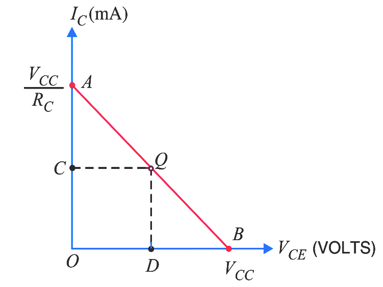
Importance. The current (IC) and voltage (VCE) conditions in the transistor circuit are represented by some point on the output characteristics. The same information can be obtained from the load line. Thus when IC is maximum (= VCC /RC), then VCE = 0 as shown in Above Fig. If IC = 0, then VCE is maximum and is equal to VCC. For any other value of collector current say OC, the collector-emitter voltage VCE = OD. It follows, therefore, that load line gives a far more convenient and direct solution to the problem.

Note. If we plot the load line on the output characteristic of the transistor, we can investigate the behaviour of the transistor amplifier. It is because we have the transistor output current and voltage specified in the form of load line equation and the transistor behaviour itself specified implicitly by the output characteristics.

Why load line ? The resistance RC connected to the device is called load or load resistance for the circuit and, therefore, the line we have just constructed is called the load line.

Don't Miss Our Updates
Be the first to get exclusive content straight to your email.
We promise not to spam you. You can unsubscribe at any time.
Invalid email address
You've successfully subscribed !

Continue Reading

Full Wave Rectifier
Transistor Stabilisation
Methods of Transistor Biasing
Transistor as Amplifier
Half Wave Voltage Doubler using Diodes
Short Circuit and Open Circuit
Share This Article
Facebook Whatsapp Whatsapp LinkedIn Copy Link
Share
Leave a Comment

Leave a Reply Cancel reply

Your email address will not be published. Required fields are marked *

Stay Connected

128.3kFollowersLike
69.1kFollowersFollow
210kSubscribersSubscribe
38kFollowersFollow

Categories

Explore More

pi filter Operation
Electronic Symbols
Types of Resistors
How the Matrix Keypad works with a Micro controller?
Basic Electronics Questions & Answers
Limitations of Resistors
How a PN Junction Formed in a Diode
Comparison of Half wave Rectifiers and Full wave Rectifiers

Keep Learning

Zener Diode Limiter Working

Zener Diode Limiter

Applications of Photo diodes

Applications of Photo diodes

Diode Rectifier

Bridge Rectifier Working Animation

Diodes Voltage Quadrupler

Diodes Voltage Quadrupler

Cathode Ray Tube Deflection System

Cathode Ray Tube Deflection System

Fluorescent Screen of CRT

CRT Fluorescent Screen

What is a Filter Circuit

What is a Filter Circuit ?

Zener Diode

Zener Diode Breakdown Characteristics

Learn More

orifice plate vent hole

What is the Purpose of Orifice Plate Drain Hole and Vent Hole?

Rotameters Working

Rotameter Working Principle and Animation

Thermocouples

Important Factors for Thermocouple Selection

Level Transmitter with Zero Suppression

DP Level Transmitters Compensation Techniques

Heat Tracing Problems

Heat Tracing Problems

Digital Electronics Multiple Choice Questions

Introduction of Arithmetic Operation

Thermal Dispersion Flow Switch Working Principle

Thermal Dispersion Flow Switch Working Principle

Digital Electronics Objective Questions

Digital Electronics Objective Questions – Set 6

Menu

  • About
  • Privacy Policy
  • Copyright

Quick Links

  • Learn PLC
  • Helping Hand
  • Part Time Job

YouTube Subscribe

Follow US
All rights reserved. Reproduction in whole or in part without written permission is prohibited.
Welcome Back!

Sign in to your account

Username or Email Address
Password

Lost your password?