A linear amplifier provides amplification of a signal without any distortion so that the output signal is an exact amplified replica of the input signal. A voltage-divider biased transistor with a sinusoidal ac source capacitively coupled to the base through C1 and a load capacitively coupled to the collector through C2 is shown in Figure. The coupling capacitors block DC and thus prevent the internal source resistance, Rs, and the load resistance, RL, from changing the dc bias voltages at the base and collector.
The capacitors ideally appear as shorts to the signal voltage. The sinusoidal source voltage causes the base voltage to vary sinusoidally above and below its dc bias level, VBQ. The resulting variation in base current produces a larger variation in collector current because of the current gain of the transistor.
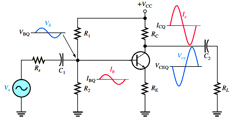
As the sinusoidal collector current increases, the collector voltage decreases. The collector current varies above and below its Q-point value, ICQ, in phase with the base current. The sinusoidal collector-to-emitter voltage varies above and below its Q-point value, VCEQ, 180° out of phase with the base voltage, as illustrated in Figure. A transistor always produces a phase inversion between the base voltage and the collector voltage.
A Graphical Picture
The operation just described can be illustrated graphically on the ac load line, as shown in Below Figure. The sinusoidal voltage at the base produces a base current that varies above and below the Q-point on the ac load line, as shown by the arrows.
Fig : Graphical ac load line operation of the amplifier showing the variation of the base current, collector current, and collector-to-emitter voltage about their dc Q-point values. Ib and Ic are on different scales.
Lines projected from the peaks of the base current, across to the IC axis, and down to the VCE axis, indicate the peak-to-peak variations of the collector current and collector-to- emitter voltage, as shown. The ac load line differs from the dc load line because the effective ac collector resistance is RL in parallel with RC and is less than the dc collector resistance RC alone.
In this post, we will learn the basic requirements for a network switch to be…
The PLC panel and MCC panel interface signals are start, stop, run feedback, trip, local…
In this article, we are going to discuss about shutter door control using induction motor…
Electrical Drives control the motion of electric motors. Motion control is required in industrial and…
PLC ladder logic design to control 3 motors with toggle switch and explain the program…
VFD simulator download: Master the online tool from the Yaskawa V1000 & programming software for…

