Semiconductor electronics is the branch of electronics that deals with devices made of semiconductor materials, usually silicon. These materials have an electrical conductivity that falls between a conductor (like copper) and an insulator (like rubber).
Semiconductor devices are essential components in modern electronic circuits and systems. They include diodes, transistors, integrated circuits (ICs), and many others. These devices use the unique properties of semiconductors to control the flow of electrical current in a variety of ways, allowing for functions such as amplification, switching, and signal processing.
Different Materials
All natural materials are classified into insulators, semiconductors, and conductors based on their electrical conductivity.
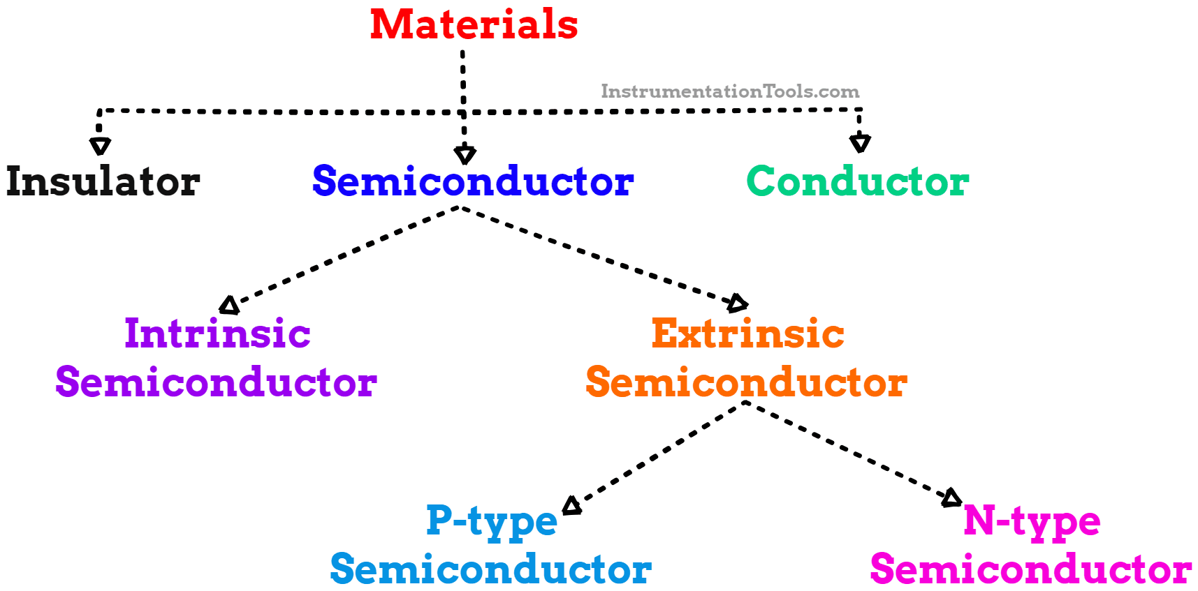
Fig.1. Classification of Materials
Energy Bands of Solids
A. Energy band gap
Energy band gap (Eg) is the minimal energy needed to move electrons from the valence band to the conduction band. It is the space between the conduction band’s bottom and the valence band’s top.
The value may vary depending on the type of material.
Eg = hv = hc/λ
λ = wavelength
h = Planck’s constant
c = velocity of light
The range of energy that an electron in a solid possesses is known as its energy band. In solids, there are two kinds of energy bands.
1. Valence Band
There are valence electrons in this energy band. Electrons can occupy this band entirely or partially, but it can never be empty. This band’s electrons are unable to obtain enough energy from an outside electric field to participate in current conduction.
2. Conduction Band
This band contains conductive electrons. This band has either no electrons or some electrons that are only partially present. Electrons in this band contribute to current conduction.
B. Forbidden Band
There is nothing in this band. A band gap is the smallest amount of energy needed to move an electron from the valence band into the conduction band (Eg).
The term “forbidden band gap” refers to the energy band that exists between the conduction band and valance band. It is the energy needed for an electron to transition from the balance band to the conduction band, or more specifically, the energy needed for a valance electron to liberate itself.
1 eV = 1.6 x 10⁻¹⁹ J
C. Fermi Energy Level
At absolute zero, the valence band’s lower energy levels are completely filled. Fermi energy is the maximum energy that an electron in the valence band can have at absolute zero, and the Fermi energy level corresponds to it.
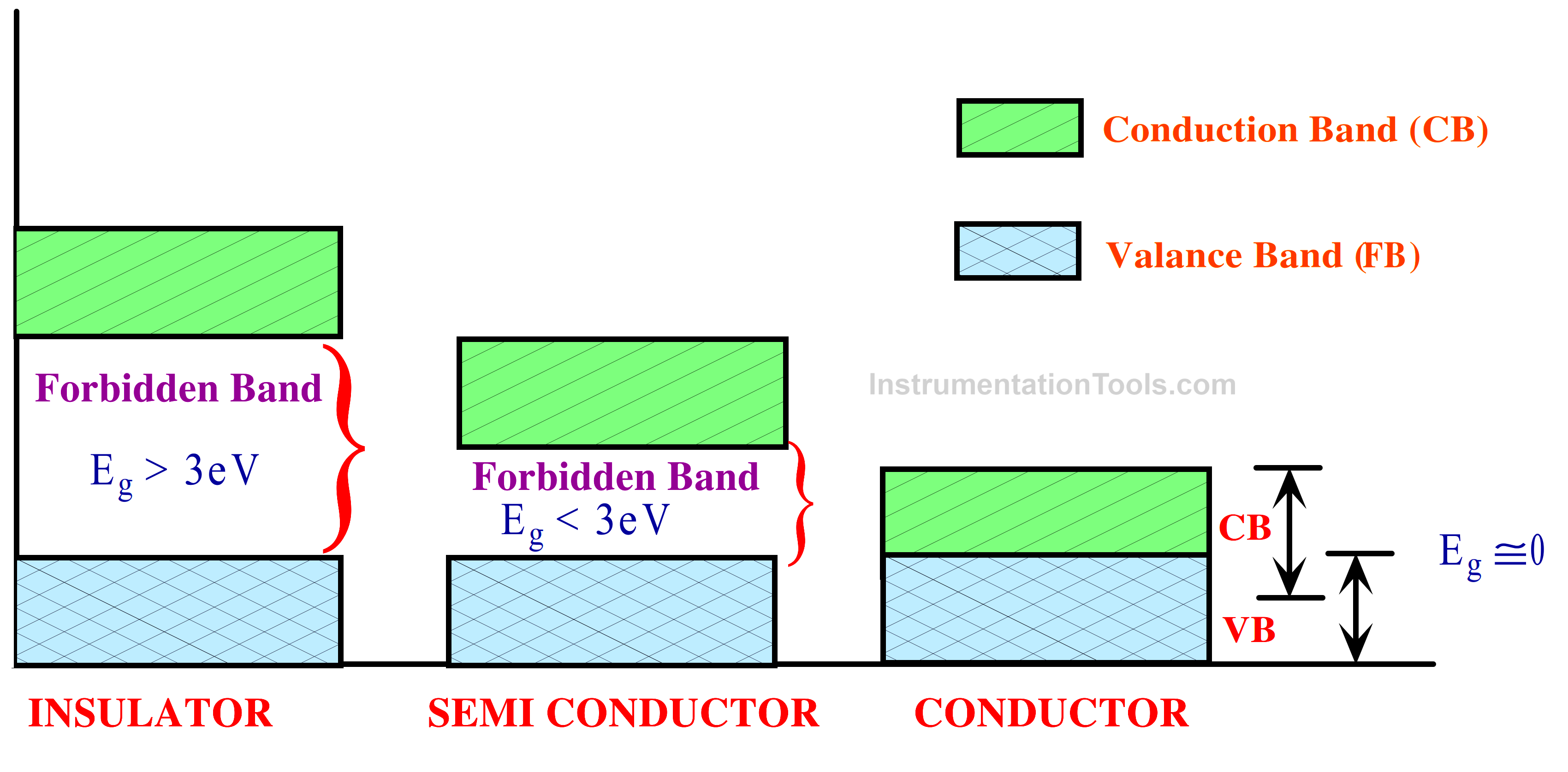
Fig 2. Energy Band of Different Materials
Classification of Material Based on Conductivity
Depending on the width of the forbidden energy band, a solid material can exhibit conductor, semiconductor, or insulator behaviour, as will be discussed below. For conductors, Eg could be nil or extremely small. It can range from 5 to 15 eV for insulators. Furthermore, the electron gap (Eg) in semiconductors is about 1 eV.
The solids are generally categorized as follows based on the relative values of electrical conductivity (σ) or resistivity (ρ = 1/σ):
(i) Conductor: They have a high conductivity and a very low resistivity.
ρ ~ 10–2 – 10–8 W m
σ ~ 102 – 108 S m–1
(ii) Semiconductors: They have conductivity or resistivity that is in between that of metals and insulators.
ρ ~ 10–5 – 106 W m
σ ~ 105 – 10–6 S m–1
(iii)Insulators: They are low conductivity, or highly resistive.
ρ ~ 1011 – 1019 W m
σ ~ 10–11 – 10–19 S m–1
A. Insulator
When voltage is applied, an insulator is a material that offers very little or No conductivity at all. For instance: Glass, Quartz, Mica, and Paper. An insulator’s typical resistivity level is between 1010 and 1012 Ω-cm.
An electron’s permitted range of energy levels is determined by a material’s band structure. The range of electron energy known as the valance band is where the electrons stay bent toward the atom and do not contribute to the electric current.
The range of electron energies above the valance band known as the conduction band is where charge can flow because electrons are free to accelerate when exposed to an external voltage source. large forbidden band gap larger than 3 eV for an insulator.
There are very few electrons in the CB (Conduction Band) as a result of this big gap, which results in low insulator conductivity. It takes more than just a rise in temperature or an applied electric field to move electrons from VB (Valency Band) to CB.
B. Conductors
When a voltage is applied across a material’s terminals, the material allows for a substantial flow of charge and is considered a conductor. i. e., its conductivity is extremely high. For instance, copper, aluminium, silver, and gold.
A conductor’s resistivity falls between 10-4 and 10-6 Ω-cm. There is an energy gap that prevents electrons from moving from the valance band to the conduction band, and the valance and conduction bands overlap. This suggests that even at zero degrees Celsius, there are free electrons in CB.
Consequently, a large current flows through the conductor at room temperature when an electric field is applied.
C. Semiconductor
A substance that falls between the insulator and a conductor is called a semiconductor. The level of resistivity lies between 10 and 104 Ω-cm. The two most often utilized are germanium (Ge=32 atomic number) and silicon (Si=14 atomic number). Everybody has four valance electrons. The band gap that is prohibited is approximately 1 eV.
For example, at absolute zero temperature (0K), the band gap energy for Si, Ge, and GaAs is 1.21, 0.785, and 1.42 eV, respectively. The electrons in the valance band lack the energy to transition from V to CB at low and zero temperatures. Semiconductors therefore behave as an insulator at 0K.
Many valance electrons gain enough energy as the temperature rises to escape the VB, cross the forbidden bandgap, and arrive at CB. Since they are able to travel around freely when an electric field is present, these electrons are now free.
Since the CB has enough electrons at room temperature, the semiconductor can conduct some current at that temperature. A material’s resistance to the flow of charge or current is inversely correlated with its conductivity.
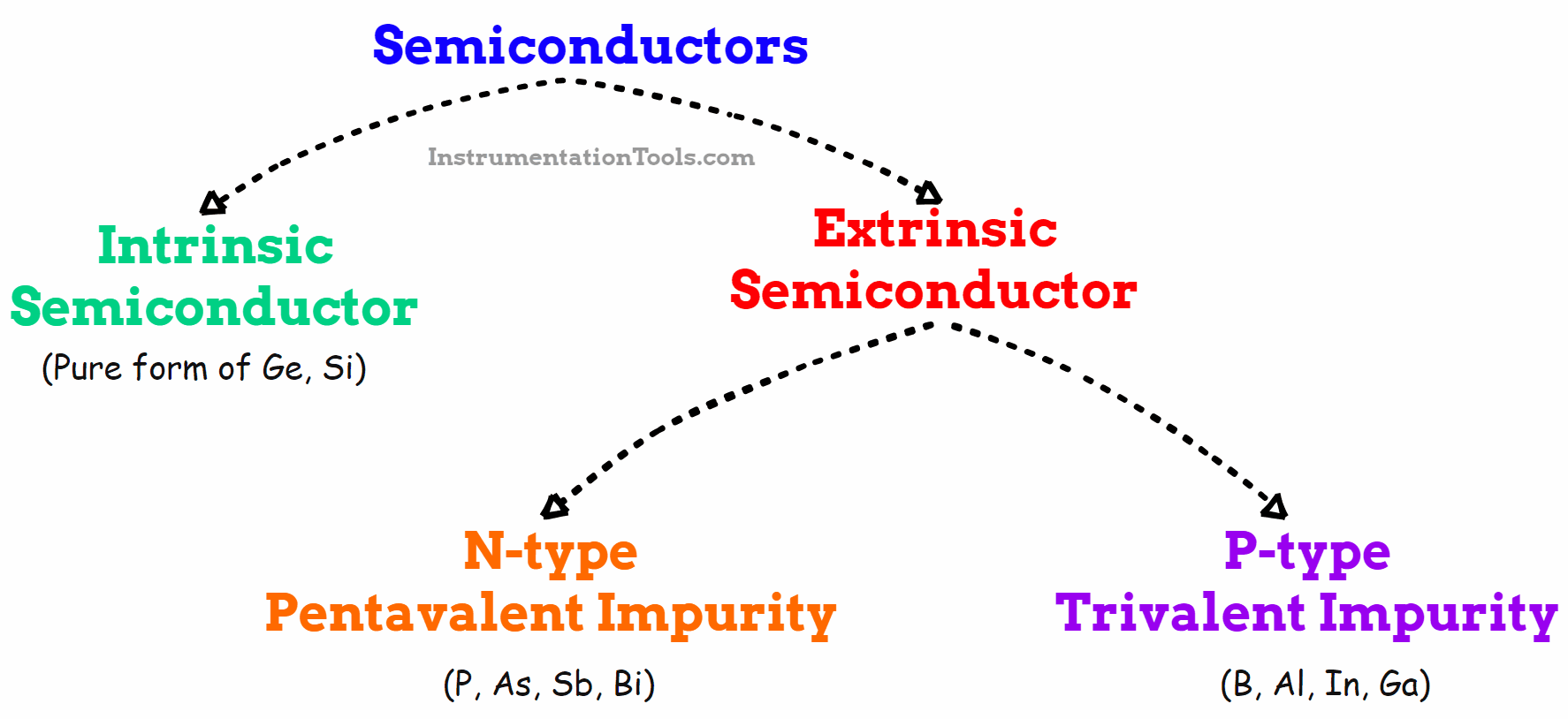
Fig 3. Types of Semiconductors
Properties of Semiconductors
The semiconductor nature of the materials cannot be determined solely by resistivity.
- Their temperature coefficient of resistance is negative. In other words, when the temperature rises, their resistance lowers.
- The addition of a suitable trivalent or pentavalent impurity significantly alters their conductivity.
Types of Semiconductors
There are two categories of semiconductors.
1) Intrinsic semiconductors
2) Extrinsic semiconductors
1. Intrinsic semiconductors
Intrinsic semiconductors are pure semiconductors such as ge and si. These materials have four electrons in their outermost orbit. To complete the octal a ge/si atom forms the covalent bonds with four other neighbouring ge/si atoms as shown in the figure.
Since there are no electrons available in the conduction band at low temperatures, the semiconductor material acts as an insulator. However, at higher temperatures, thermal agitation causes some of the covalent bonds in the semiconductor material to break, which results in the creation of an electron-hole pair.
The electron is now available in the conduction band even at room temperature and the hole is available in the valance band. The hole is a vacancy created in the valance band filled by the neighbouring electron and thus electron and hole start flowing in the valance band and due to both electron and hole electric conduction in the material is now possible.
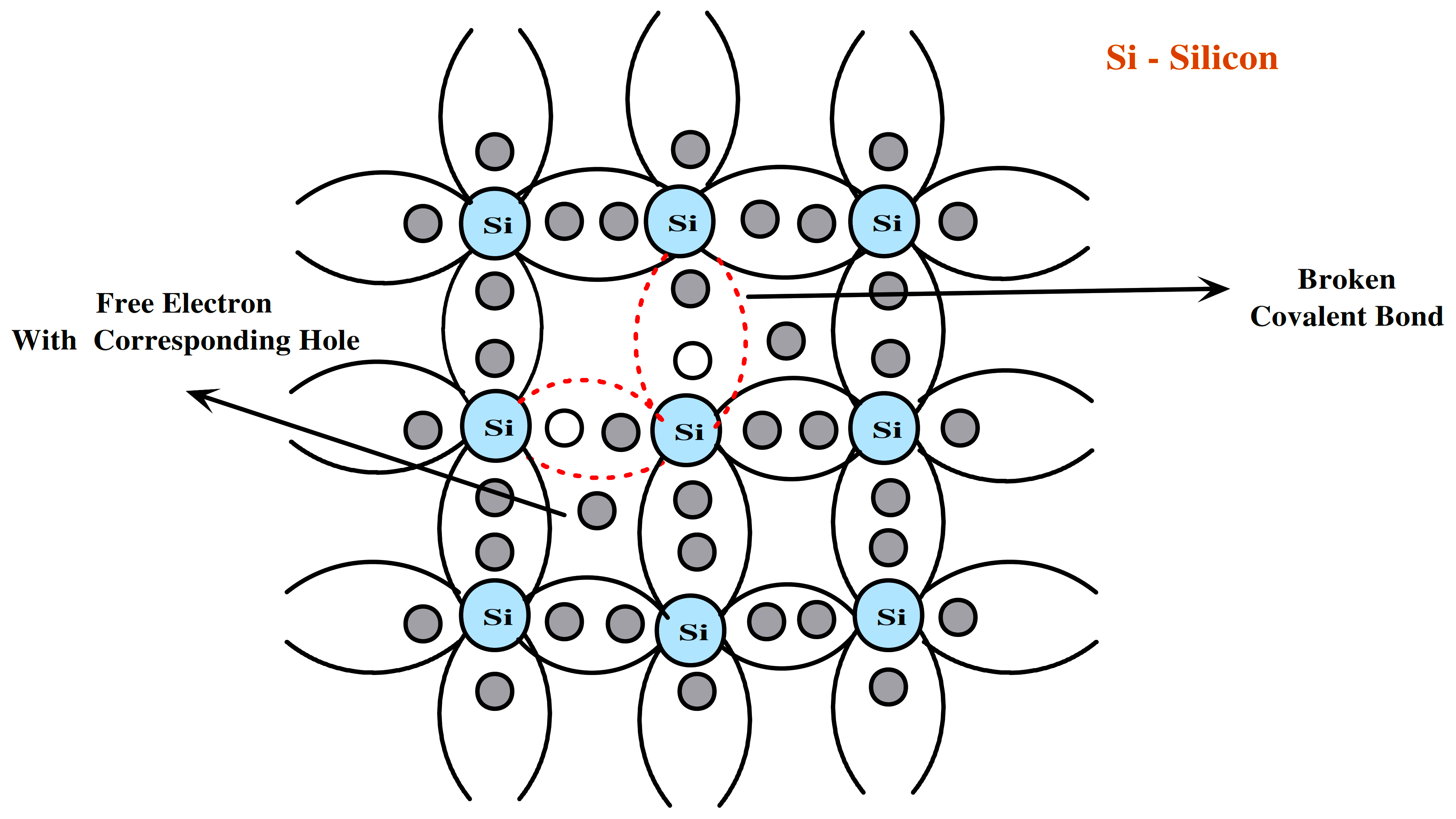
Fig 4. Crystal Structure of Si
2. Extrinsic Semiconductors
Extrinsic semiconductors are those that have been doped with impurities to change the number and type of free-charge carriers. An extrinsic semiconductor is one that has been doped, meaning that a doping agent has been introduced into it, resulting in different electrical properties than the intrinsic (pure) semiconductor.
Doping is the process of adding dopant atoms to an intrinsic semiconductor, changing the semiconductor’s electron and hole carrier concentrations at thermal equilibrium. The dominant carrier concentrations in an extrinsic semiconductor determine whether it is an n-type or p-type semiconductor. Extrinsic semiconductors are necessary components in many electronic devices due to their electrical properties.
A pure or intrinsic conductor contains thermally generated holes and electrons. However, they are relatively few in number. The controlled introduction of impurities into the semiconductor can result in an enormous increase in the number of charge carriers. The end result is the formation of an extrinsic semiconductor. This process is known as doping.
There are two kinds of impurities: donor impurities and acceptor impurities. Donor impurities consist of atoms (such as arsenic) with five valence electrons. Acceptor impurities are composed of atoms (such as gallium) with three valence electrons.
Doping involves two different types of dopants:
- Three-electron trivalent elements, such as aluminium (Al), boron (B), and indium (In), etc.
- (ii) pentavalent, or having five electrons, such as arsenic (As), antimony (Sb), phosphorous (P), etc.
N-type semiconductors
When pentavalent impurities (P, As, Sb, Bi) are added to a pure semiconductor (Si or Ge), four of the five impurity valence electrons participate in the covalent bond, encircled by four silicon atoms, while the fifth electron is released.
Donor impurity (N0) is the term for these impurity atoms that donate free electrons for conduction. Donor impurity free e- increases significantly, which is why it is a “N” type semiconductor. According to semiconductor terminology, “holes” are referred to as “minority” charge carriers and “majority” charge carriers are electrons.
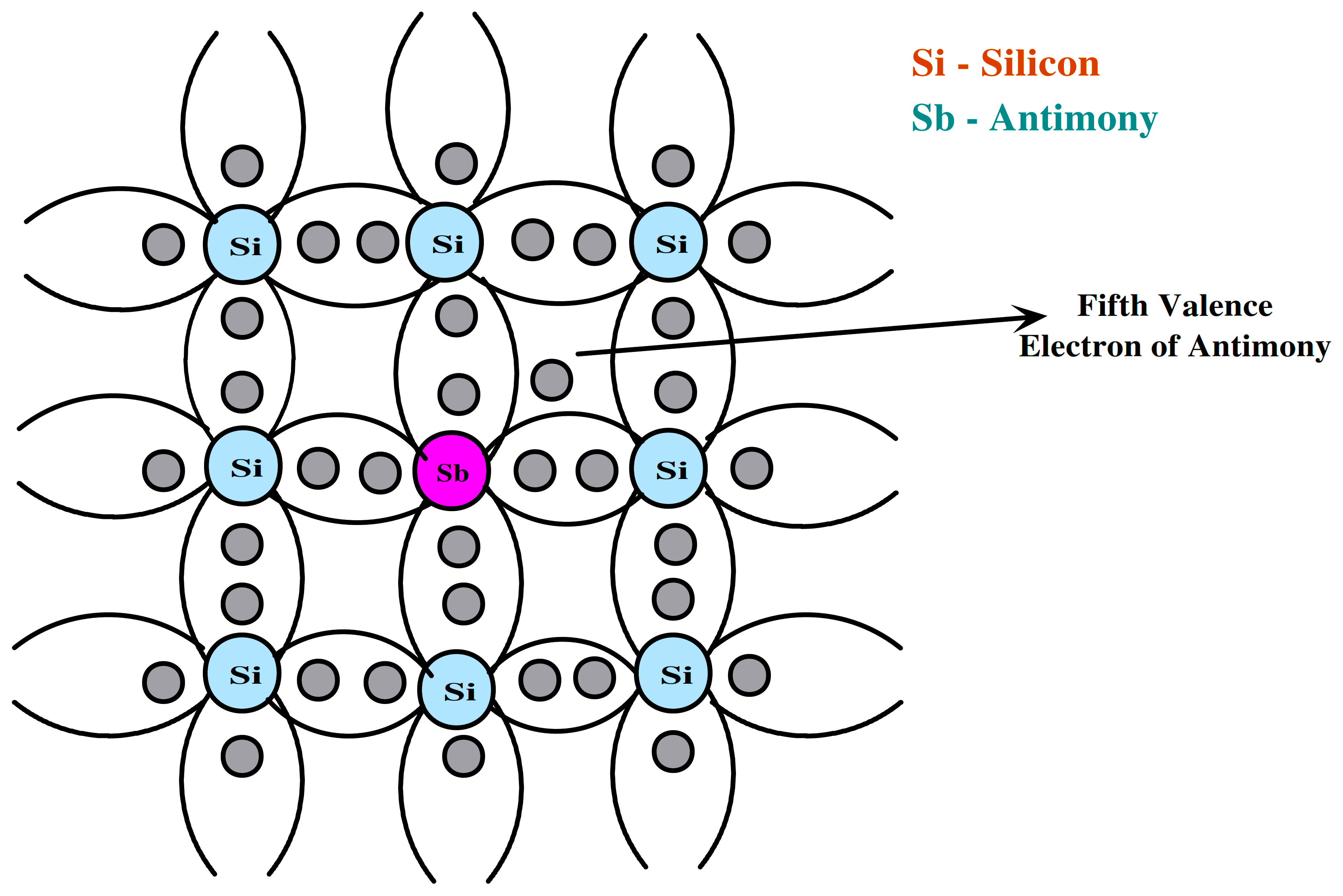
Fig 5. Crystal Structure of N-type Semiconductor
P-type Semiconductors
When a pure semiconductor (Si or Ge) is doped with a trivalent impurity (B, Al, In, Ga), the impurity’s outermost three electrons in the valence band participate in covalent bonds with the four surrounding silicon atoms, with the exception of one electron that leaves the semiconductor and creates a hole in it.
These impurity atoms are referred to as acceptor impurities (NA) when they take in bound e-from the valance band. Here, the impurity ions are referred to as “Immobile Acceptor negative Ion” and the holes are very abundant; hence the semiconductor is referred to as a “P” type. Free electrons are referred to as minority charge carriers in P-type semiconductors, while holes are referred to as majority charge carriers.
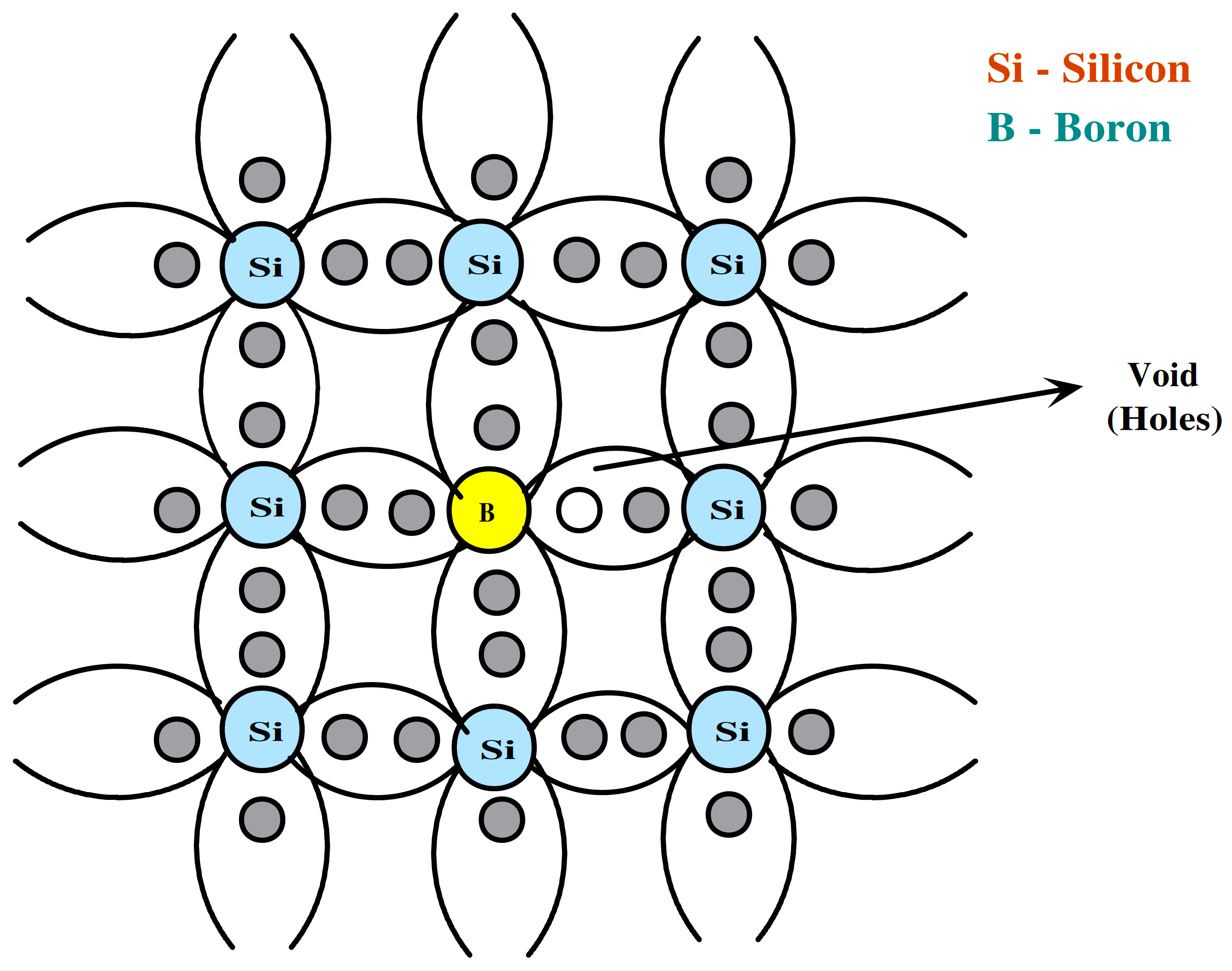
Fig.6. Crystal Structure of P-type Semiconductor
Conduction in Semiconductors
Conduction is carried out through the drift and diffusion processes.
- Drift process
In the conduction band of a semiconductor, electrons travel from the external circuit, and holes travel in the valence band.
- Diffusion process
Diffusion process is the movement of electrons from gradients of higher concentration to gradients of lower concentration.
References:
- Semiconductor Electronics, A. K. Sharma, New Age International, 1996.
- A Text Book of Electronic Devices & Circuit, J. B. Gupta, S.K. Kataria & Sons.
- Electronic Devices and Circuits 5Th Edition by S Salivahanan, Mc Graw Hill India.
- https://ncert.nic.in.
