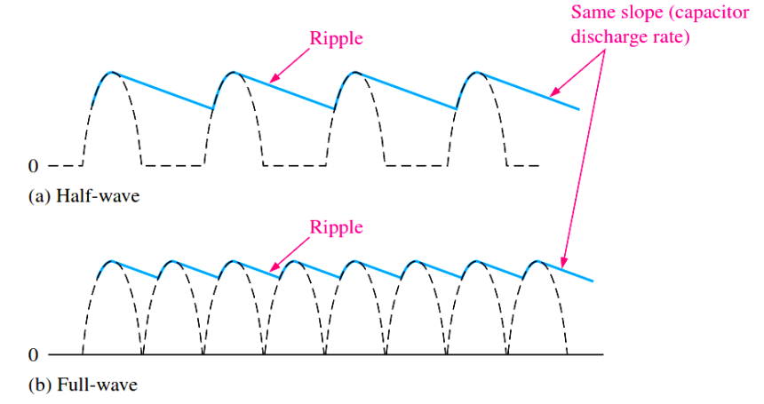
Ripple Voltage in Rectifiers
Ripple Voltage As you have seen, the capacitor quickly charges at the beginning of a cycle and slowly discharges through RL after the positive peak of the input voltage (when the diode…
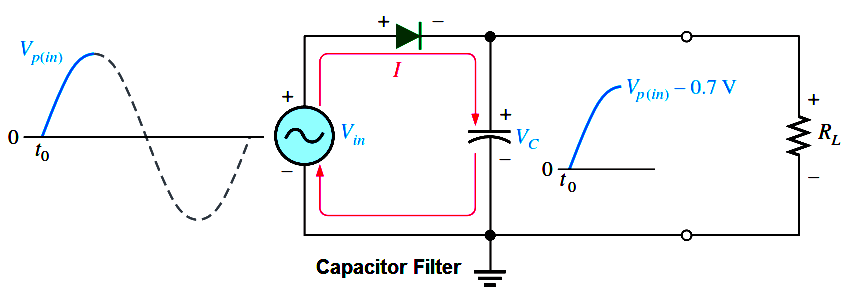
Capacitor Filter Working Principle
A half-wave rectifier with a capacitor-input filter is shown in Below Figure. The filter is simply a capacitor connected from the rectifier output to ground. RL represents the equivalent resistance of…
Full Wave Bridge Rectifier Peak Inverse Voltage
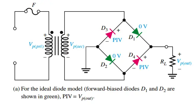
Peak Inverse Voltage Let’s assume that D1 and D2 are forward-biased and examine the reverse voltage across D3 and D4. Visualizing D1 and D2 as shorts (ideal model), as in Figure (a),…
Full Wave Bridge Rectifier Operation
The bridge rectifier uses four diodes connected as shown in Figure. When the input cycle is positive as in part (a), diodes D1 and D2 are forward-biased and conduct current in the…
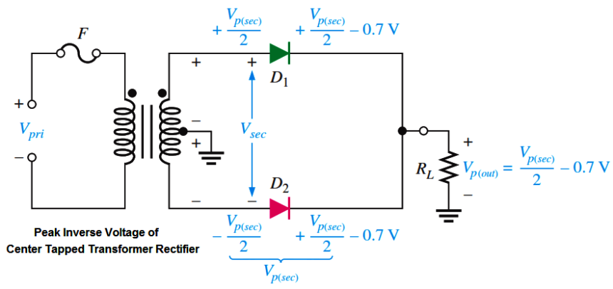
Peak Inverse Voltage of Center Tap Rectifier
Peak Inverse Voltage Each diode in the full-wave rectifier is alternately forward-biased and then reverse-biased. The maximum reverse voltage that each diode must withstand is the peak secondary voltage Vp(sec). This is…
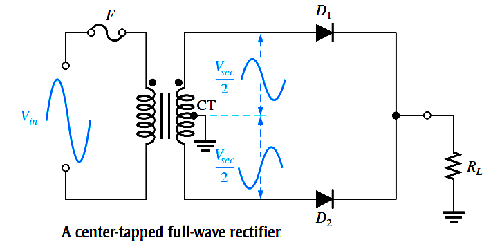
Center Tapped Full Wave Rectifier Operation
A center-tapped rectifier is a type of full-wave rectifier that uses two diodes connected to the secondary of a center-tapped transformer, as shown in Below Figure. The input voltage is coupled through…
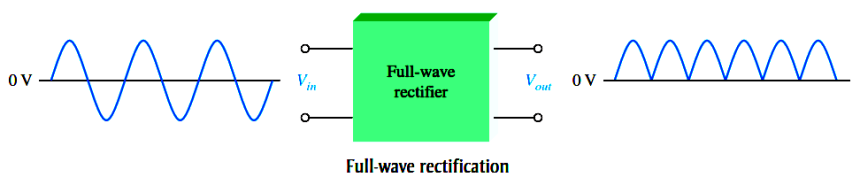
Full Wave Rectifier
A full-wave rectifier allows unidirectional (one-way) current through the load during the entire 360° of the input cycle, whereas a half-wave rectifier allows current through the load only during one-half of the…
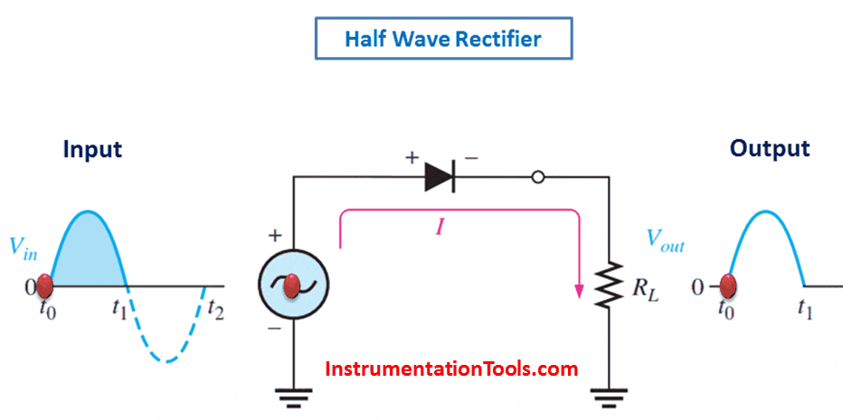
Half Wave Rectifier Principle
Half Wave Rectifier : Half-Wave Rectifier Operation The below Figure illustrates the process called half-wave rectification. A diode is connected to an ac source and to a load resistor, RL, forming…
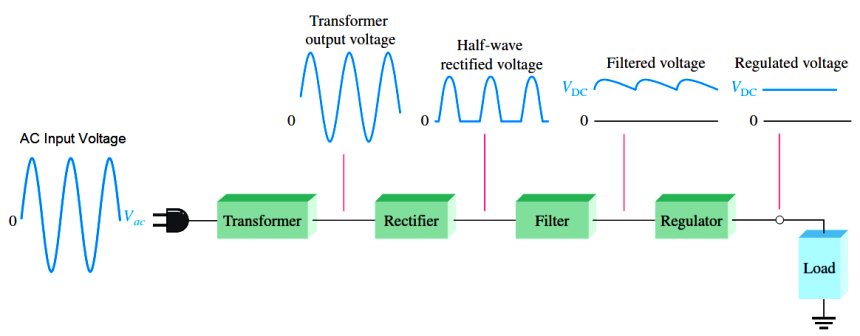
Basic DC Power Supply Circuit
All active electronic devices require a source of constant dc that can be supplied by a battery or a dc power supply. The dc power supply converts the standard AC voltage available…
Difference between ideal diode & conventional diode
An ideal diode is a diode that acts like a perfect conductor when voltage is applied forward biased and like a perfect insulator when voltage is applied reverse biased. So…
